The hardware
For the final hardware, I wanted the following features, so I designed the electronics to support them:
- Both main and backboard LCDs, with the main LCD running at full 60FPS
- Internal speaker for sound effects and music
- Haptic feedback so I can feel the (virtual) ball bouncing around on the table
- Actual plunger (with analog feedback to the microcontroller) to launch the ball
- Pinball-like flipper buttons
- LiIon battery so you can play the game while it's stood comfortably on a table

The heart of the table is an ESP32S3-Wrover module. It has 8MiB of flash as well as 2MiB of PSRAM integrated in the module. It is a module capable of WiFi/BTLE, and the antenna for that is still there, but it's only used for its processing power here. Most of the IO consists of the parallel interface to the main LCD. There's also a SPI bus which is used by both the main LCD to set up parameters as well as the high-speed data bus to the secondary backbox LCD. The backbox LCD is actually on a separate PCB with its own backlight logic.

That display doesn't need that much more than those IO signals and a 3.3V voltage. It's somewhat odd in that it also needs a pretty high 12V for the backlight, though. For this, there's a boost converter. I thought I would be smart and make this into a current source: in its current configuration, it generates whatever voltage is needed to push 20mA through the backlight LEDs. While testing, I found that this had a flaw: if the LCD is not connected, it still drives up the voltage to push 20mA through... meaning the voltage goes up and up and up, until a component fails. A hastily bodged in 15V zener fixed this issue.

The main power supply. It is based on a LiIon battery, connected to J4. This battery has internal protection, so that's not in this schematic. It needs to be charged every once in a while, and I used a TP4056 for that. It also turns out it's not a good idea to run hardware off a LiIon you're charging, as the charger chip can't use the charging current to make decisions about the status of the LiIon cell. To get around this, Q1 and D3 are used; this shunts the 5V from the USB connector straight into the power supply for the rest of the logic (VBAT) so the device can both charge and be played. This means I needed to keep in mind VBAT could have a voltage of up to 5V. The USB port is also hooked up to the native USB pins of the ESP32S3 to make flashing easy without needing any extra hardware or to open the enclosure.

This is the audio amplifier. Unlike the ESP32, the ESP32S3 does not have an internal DAC, but I use the fact that it has a PDM mode. This outputs high and low signals at a very high speed, with the average being the audio signal: it is somewhat like PWM but without the fixed PWM frequency. Normally, you would want to use a lowpass filter before actually feeding that signal to an amp. I did not do this, which likely will cost me some energy efficiency as the higher modulation frequencies are still sent through the amp and the speaker, even if they're inaudible.

Haptic feedback is delivered by two linear actuators, the same style as nowadays is used in high-end mobile phones. These effectively are coils that move a weight on a spring back and forth: because Newtons 3rd law, the weight also moves the case of the actuator. As that is firmly embedded in the pinball table case, you can feel the weight being moved around. In this case, the coils of the two actuators are driven by two BD6122 motor drivers, which in turn are controlled using the MCPWM peripherals of the ESP32S3. The cheapest source of the actuators themselves actually turned out to be spare parts for those mobile phones: the ones I used were from dismantled Huawei Mate 30 Pro phones and cost me the equivalent of USD1.50 per unit.

The start buttons as well as the left and right flipper are connected to the ESP32S3 via an I2C port expander, as I ran out of GPIOs. The port expander also controls the reset signal for the LCDs. The buttons themselves are non-clicky linear microswitches. This is to emulate how pinballs work: the flipper buttons that those have have a pretty mushy feeling, but because they actuate the flippers using some pretty powerful electromagnets, you get the haptic feedback that way. I wanted to have the same effect with the linear accelerators.

Because I had the I2C-bus anyway, I also added an accelerometer: this way you can bump the pinball machine and it actually moves the ball and tilts the machine if you do it too often.

I wanted to have analog feedback on the plunger as well, but as I designed this during a lockdown and parts were pretty hard to get to, I needed to use a sensor for this that I already had on hand. Because of this, I made a bit of an odd choice: the plunger mechanics consist of a rod and a spring, like a real pinball machine, but rather than hitting the ball, it hits... an 0805 10uF MLCC capacitor. You may not know it, but the material those caps are made of are a little bit piezo-electric, meaning they generate a voltage when being flexed or hit. It took some time to get this effect working correctly, as a capacitor needs to be poled for this to fully work and the literature around this is pretty academic. I found it works without this process if I simply bias the capacitor with a fixed voltage.
This schematic, then, is a combined amplifier and peak detector. R6 biases the capacitor, and when it is hit by the plunger snapping back, the extra voltage is passed through C10 to opamp U6. This opamp is configured as an ideal diode which charges C12. R8 and R9 have a dual use: they both set the opamp to also amplify the input signal, as well as slowly discharge C12 after it has been charged. All this means that when the plunger hits the MLCC capacitor, the voltage on C12 will peak and will hold there for a while, long enough for the MCU to measure it using one of its ADC channels.
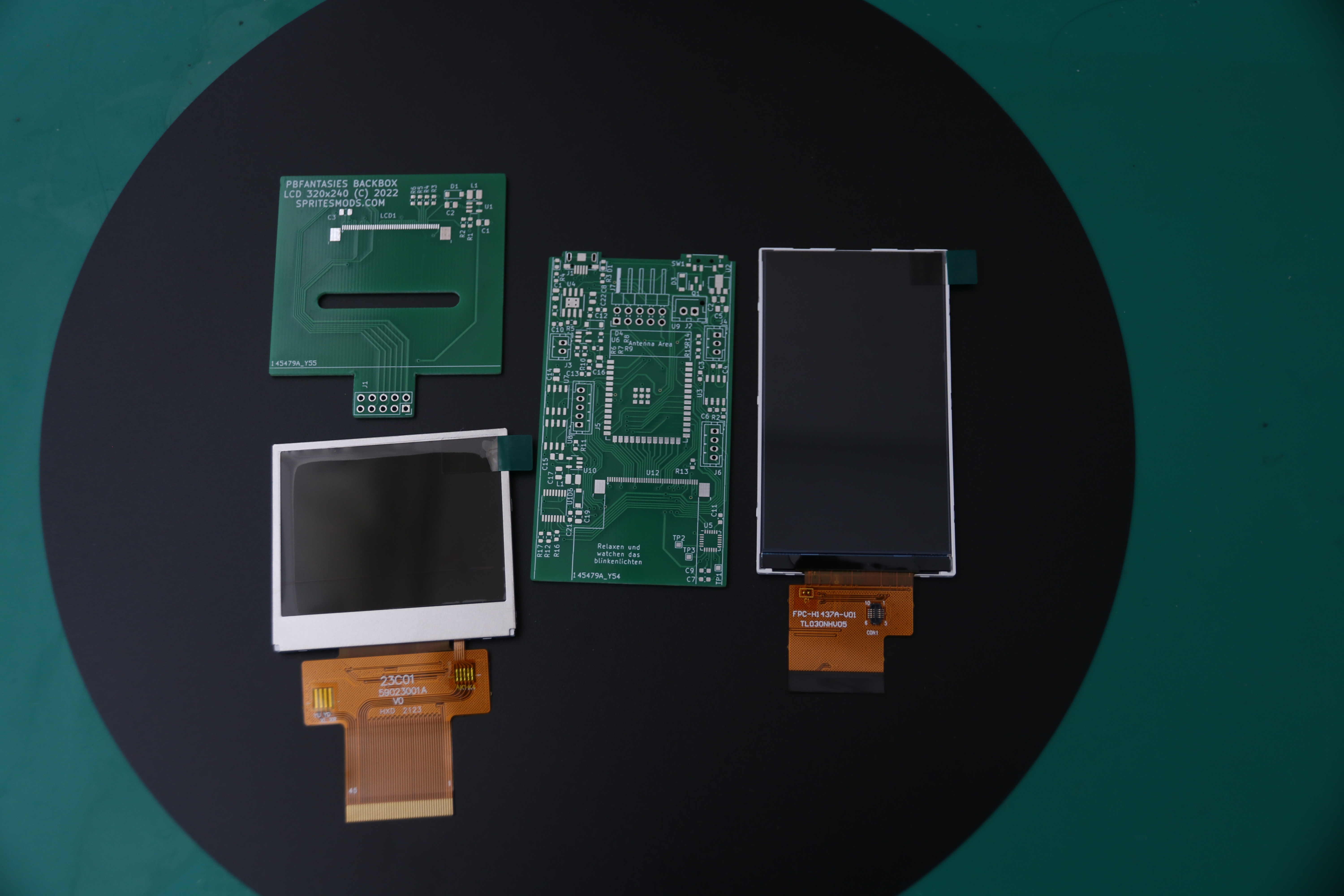
I quickly did the layout the PCBs; they're both of such a size that they can go behind their respective LCDs, with only the connectors and the power switch sticking out. They're double-sided PCBs, so I could make them for cheap at a random board house. Note that while I put an ESP32 with WiFi on there, I have no intention to use the WiFi, which allowing me to put the ESP32 in a position that would otherwise be horrible for radio reception. Don't take this as a good example if you want to design a board that does actually need WiFi/BT connectivity!
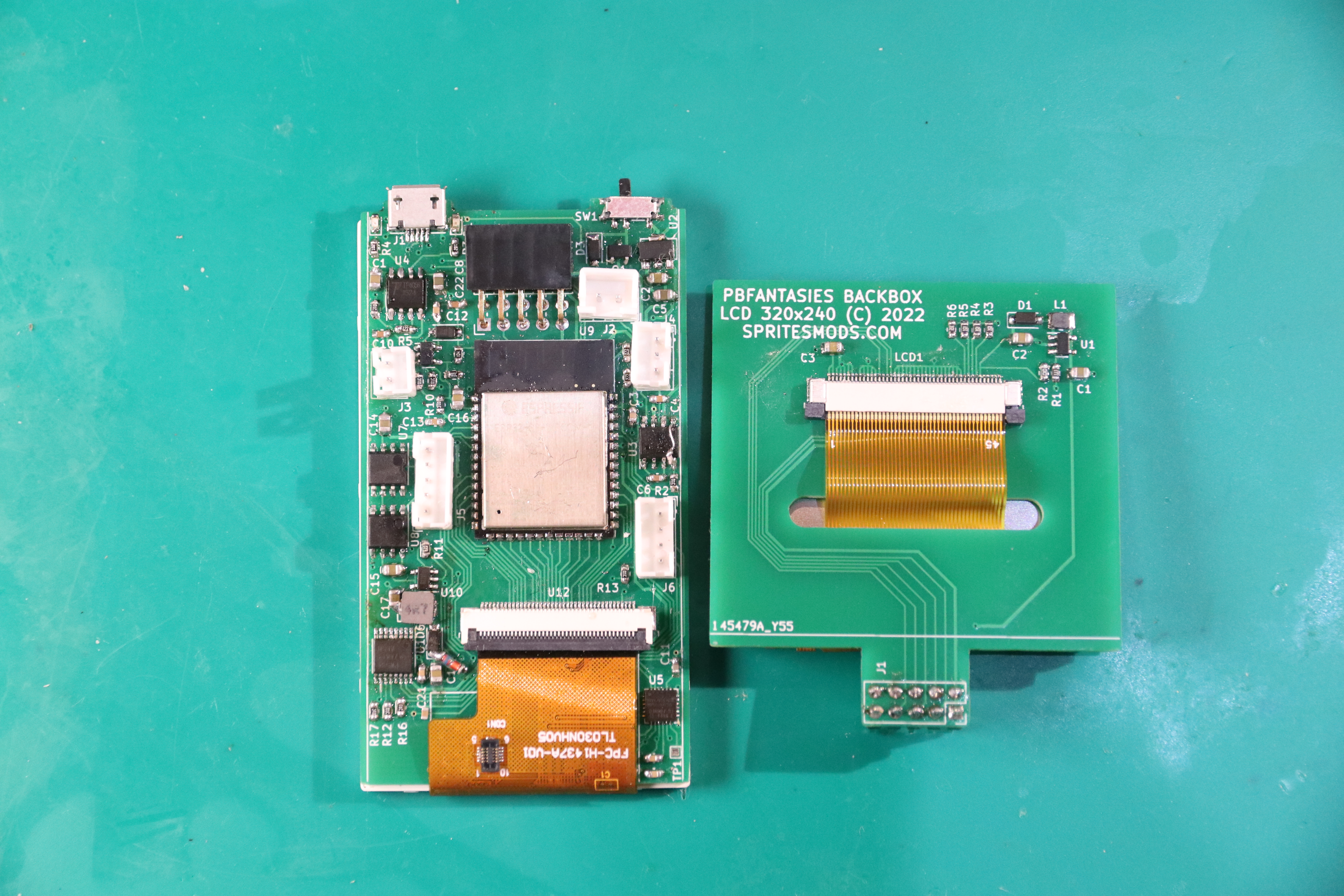
The assembled PCBs. Note that aside from the snafu in the backlight converter of the main PCB, I also needed to bodge in a resistor I forgot in the audio circuit. I fixed these two things in the PCB artwork that I made public.
Now all I needed was to put them into a case... a case which I would need to design first.