Figuring out the ISA
As I already expected, the case of the camera has the size it has mostly because it makes it fit in a kids hand easily and not because the internals take up so much space: much of the interior of the case is empty. I already didn't expect much, but the main and selfie camera module were even smaller than I thought; absolutely miniscule. Besides the camera modules, a tiny PCB with a LED for the flash and a speaker, all that was in the case was an LiIon pouch cell battery and the main PCB with the LCD connected to it.


The main PCB was pretty barren. It contains connectors for all the external components as well as all the buttons to control the camera. For connectivity, it also carried the USB port and the micro-SD-card slot. It's also got the standard supply of active components: a SOT23 LiIon charging IC and a 3.3V regulator in SOT23-5 packages. There is some flash in the form of a 4MiB Spansion S25FL132K SPI flash chip, and all the rest is done by the main chip, a HX-Tech HX3302B.
This chip is just about the most unknown chip on the Internet. At the time of writing, the term "HX3302B" in quotes only hits two Aliexpress pages which sell a camera with this as the "main control scheme", two pages which enumerate lots of IC codes without adding info, and one Twitter mention of some Japanese person who also opened up a camera like mine and spotted the chip. Even the name of the company, HX-Tech, only seems to turn up false positives.
So we're dead in the water, perhaps? An unknown chip, with an unknown architecture, no known ways of debugging it or interfacing to it... There's not even a debug serial port I can find: while a testpoint is labeled TX, it goes to the line used for the SD card activity LED and there is no serial data on it. Perhaps they ran out of GPIOs and this pin only carries an UART signal when you load up some special debugging build of the firmware. But wait, there still is that 4MiB flash chip, maybe that can shed some light on things?

Reading the flash and running it through the usual tools reveals that we may be in luck:
- There seems to be firmware in there, and it's not encrypted or compressed.
- The firmware actually does have a fair few debug strings embedded in it.
- Changing one of the strings and flashing the code back indicates there's no cryptographic hash or even CRC being checked. If we know what to modify, having the camera accept the modification is trivial.
There's also some bad news:
- No indication on how to turn on a debug UART.
- No hint of what architecture this chip is... just that it's in the HX330x family, something which also doesn't give any useful results when you throw it into a search engine.
- Strangely, even automated tools cannot tell me what ISA the CPU inside the chip is. Cpu_rec gives me the command line equivalent of a blank stare, while isadetect gives varying guesses with extremely low confidence.
- Even manual checks against some ISAs I know of but are not part of those tools (e.g. OpenRISC, some Sunplus architectures) fail.
Now I'm not against reverse engineering an ISA from scratch, but I needed a bit more to go on that just the raw binary. Knowing what areas of the binary were instruction would already help, as well as roughly knowing what areas were used for what. The main SoC needs to load the information from flash anyway, so why not hook that up to a logic analyzer and see what it does? Perhaps we can see what bits are loaded on startup; that would limit the space we need to look at by a lot already.
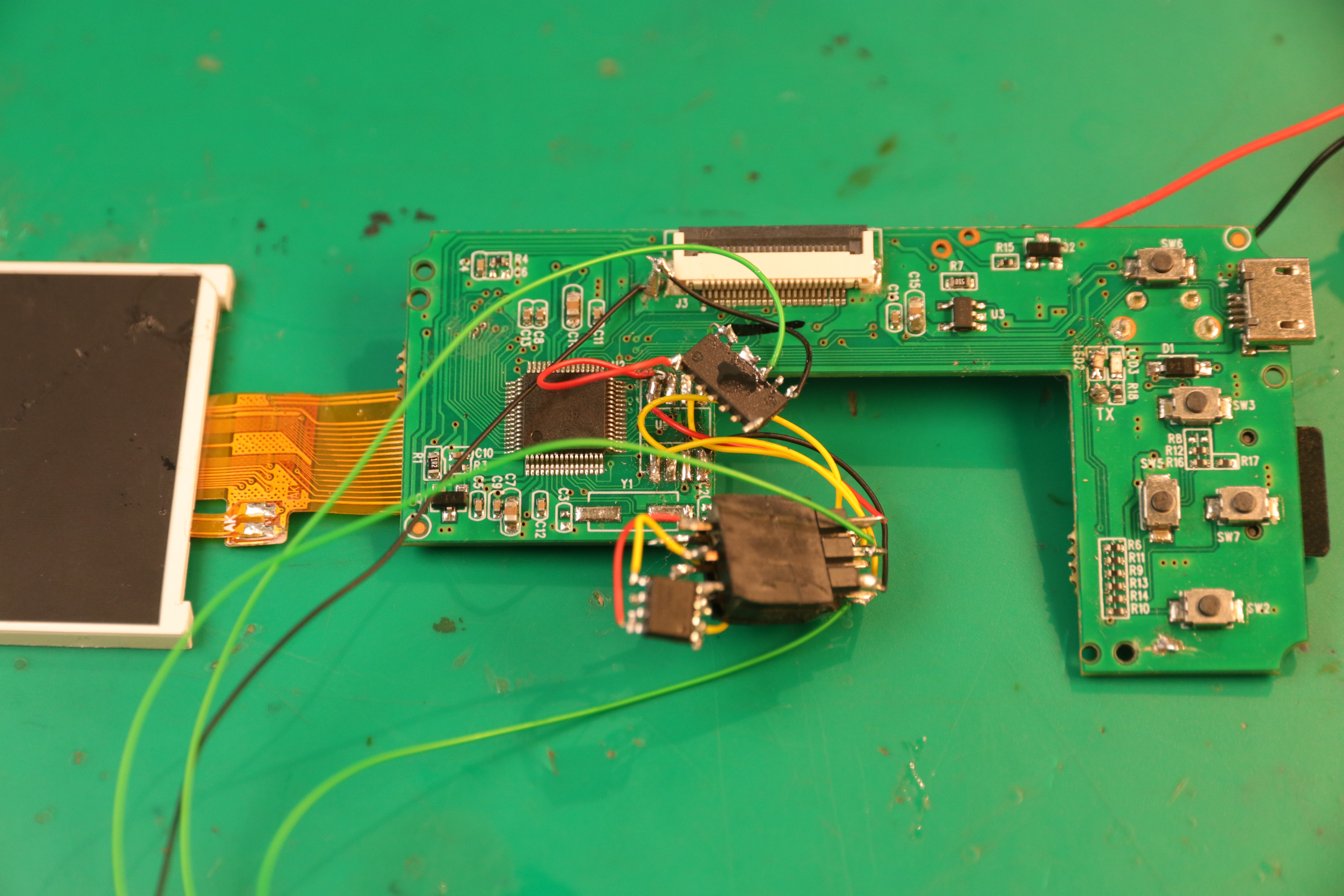
As the PCB combines MOSI and MISO of the flash chip, I only needed to hook up three wires plus a ground. However, I did not get good captures from this, plus the device failed to boot every now and then. As it turned out, the CLK line of the chip is pulsed at something like 70MHz, and the added capacitance of the LA probe deteriorated the signal too much to work. To fix this, there's a 74LVC00 connected as a simple buffer between the CLK line and the LA probe. Also note that I relocated the flash to a 6-pin header to make it easier to take it out and read or reprogram it.
Like all modern logic analyzers, the software that came with mine had no issues decoding the SPI signal into flash commands.

Simplified, here's what happens:
- The chip reads 512 bytes from address 0
- The chip reads 10752 bytes from address 0x20
- The chip 34816 bytes from address 0x2c00
- Lots of 4-byte reads from flash, mostly to consecutive addresses but sometimes the address 'jumps'
- Then something changes and there's only 16-byte reads
I have some experience with chips that boot from external flash, so I can hazard a good guess to what's happening here:
- The first 512 bytes is a header of sorts: it indicates which sections need to be read into RAM.
- The following two large reads do exactly that: copy a chunk of flash to RAM in order to be able to run it there.
- The 4-byte reads look like the CPU is executing directly from the memory-mapped flash, reading one instruction at a time, mostly simply going to the next instruction but sometimes looping, jumping to a subroutine etc. The fact that these reads are always 4-byte hints at a 32-bit CPU.
- As running directly from flash is inefficient, there's a cache that gets initialized later on. The cache line size of that is 16 bytes, so we only see reads of that size and only for newly-accessed addresses.
The 4-byte reads are actually very useful here, as they show the program flow, and by looking at where the flow jumps to a non-sequential address, I can already decode some program flow instructions.
This allows me to already detect subroutines and jumps in the code, which is an useful start. However there are just 100 or so 4-byte reads before the cache gets enabled, and enabling the cache effectively makes following the trace impossible. But what if I could stop that? In the original source, enabling the cache is probably done using a `enable_icache()` subroutine or something, so what if I nerfed the last 'call' instruction before the cache was enabled?
One hexedit, flash programming operation and LA trace later, I had my answer in the form of a 300MiB file detailing exactly what instruction the CPU was fetching for the entire startup process. Great, now to make use of that to decode even more instructions.
One of the things that the firmware did have that was immediately obvious were debug printfs. As the UART itself didn't seem to be mapped to any string, I couldn't read the messages that were being sent, but I could see that they were read in the printf function. Now, the nice thing about the printf function is that there's not that many ways to implement it, so its structure generally is the same amongst all CPUs: read a byte, compare with the '%' character, output if it is not, interpret the character behind it if it is. Because the structure is so well-know and I could correlate the program flow with the hex instructions in flash, this divulged a lot of instruction types: memory loads and stores, register-to-register transfers, offsets, details about register compares and so on. I was sure I could have a large part of the ISA documented in no time. I was wrong about how fast my process would go, though.
My way of documenting the instruction set I had decoded, was to build a Ghidra processor definition. The advantage of doing so is that the more instructions you decode, the better the Ghidra decode gets, and as a result the easier decoding more instructions is. However, the P-code language these processor definitions are written in are quite powerful (if you write them correctly, Ghidra can properly do its decode-assembly-to-pseudo-C-trick) but also non-trivial. At some point I needed to look up how to do something, and I decided to open an OpenRisc-1000 (OR1K) definition I downloaded earlier to check how to do that... and suddenly, a lot of things in that definition struck me as oddly familiar.
Turns out that the OR1K CPU architecture really, really wants to be big-endian, and that is how 99% of the actual implementations have it. However, there is a note somewhere that if you really need to, you can add a databus scrambler to the core to make it little-endian, and it seems that is what the fine people designing the SoC in this camera did. However as this was pretty uncommon, nothing detected the binary as a known ISA. Luckily, it was trivial to add a little-endian variant of the OR1K processor to the package, and suddenly Ghidra could decode the entire binary just fine.