Final PCB
Ofcourse, If I wanted the clock radio to work for another 15 years, a wiring mess wouldn't do: a nice PCB had to be designed. The idea is to replace the old 90's PCB for a newer one, that could interface to the clock radio and the transformer in the same way the old one had.

First things first: I had to know how to position the OLED display. As you can see, it's slightly bigger
than the space for the original LED display. Nothing a little slicing of the plastic can't fix.
And something that kind-of surprised me: this is the 'before' picture. Seems like that when the clock
radio was produced, the initial designs called for a smaller display. My guess is that they sourced a
bigger one later on, but couldn't be arsed to change the moulds for the enclosure. That means someone
had to modify each and every one to fit the larger LED display. I'm just continuing that tradition.
Things like the precise position of the buttons are quite hard to measure. My solution to make it all fit
was to try to measure everything as well as I could, then design a PCB to fit these measurements.
I then converted the PCB design to a SVG file and sent it to my lasercutter. The lasercutter
cut out a piece of acrylic sheet in the shape of the PCB with the holes for the buttons drilled. I could
check if everything fits correctly, and modify the component placings if needed.

And after a few prototypes, everything seemed spot-on. I would just need to trim some plastic off the
button posts because the buttons I use are slightly bigger than the original solution.
When everything fitted, I went and designed the rest of the PCBs. I actually sent the PCB designs out a
bit prematurely, because I had an upcoming holiday and I wanted to have the PCBs when I got back. This
unfortunately meant some things were a bit less polished than I wanted. Still, after my holiday, these
beauties arrived on my doorstep:
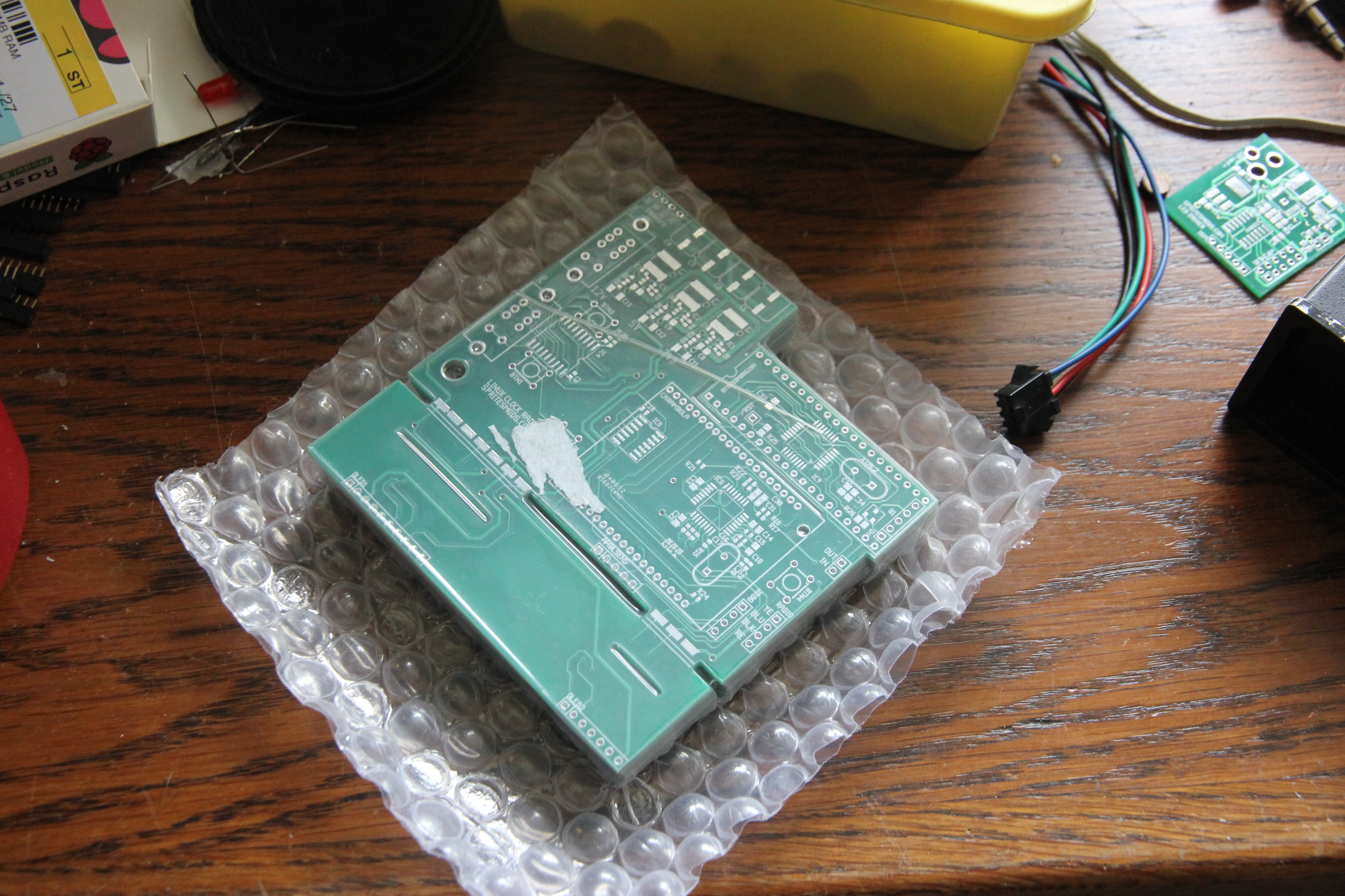
And this is one single unpacked PCB:
Disregard the small 40-pin DIP PCB in the top left corner, it's a small design for another project I
sneaked in on the same order. While it's usually forbidden to do two designs in one file, most Chinese
manufacturers will let it pass if you have some PCB traces running between them.
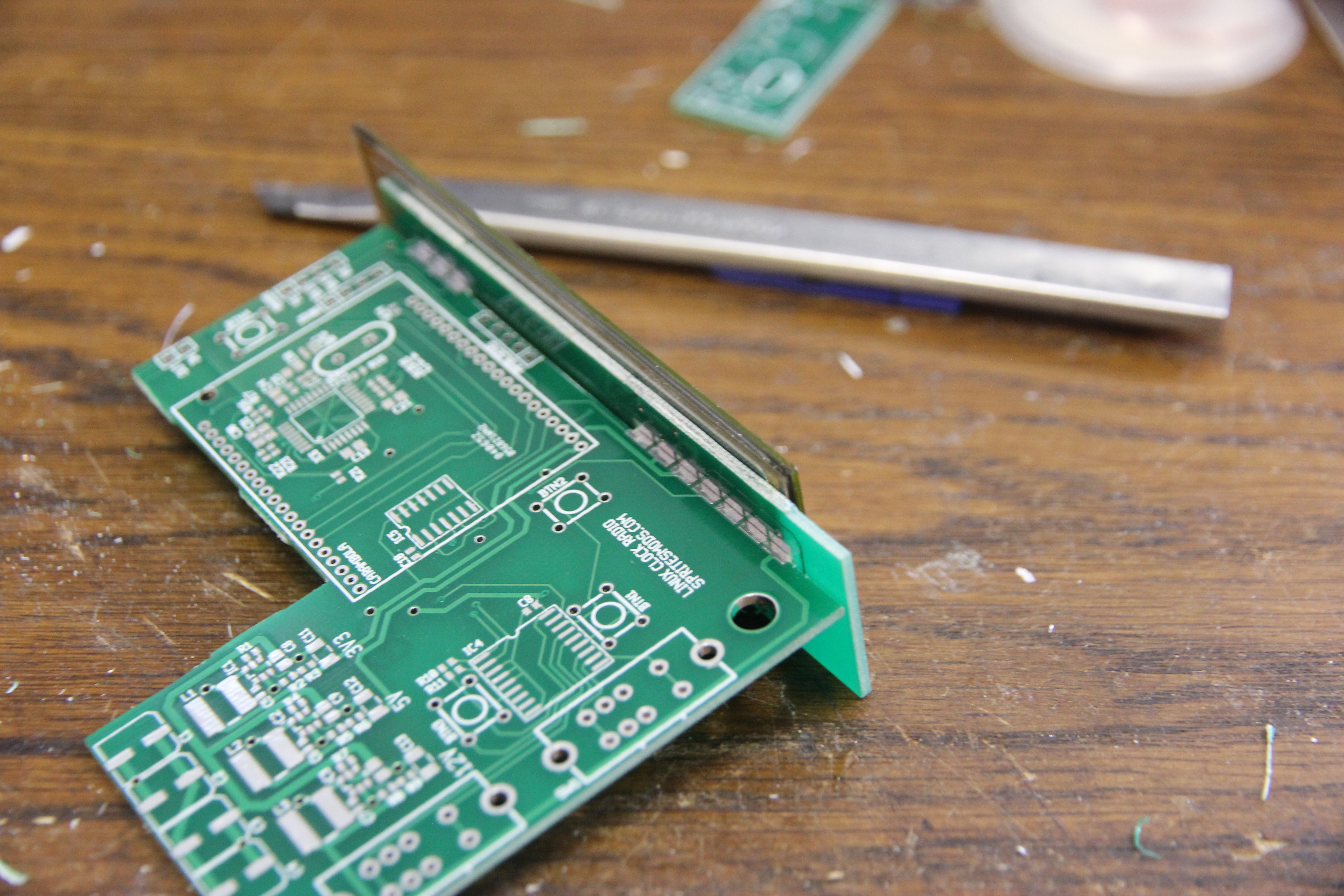
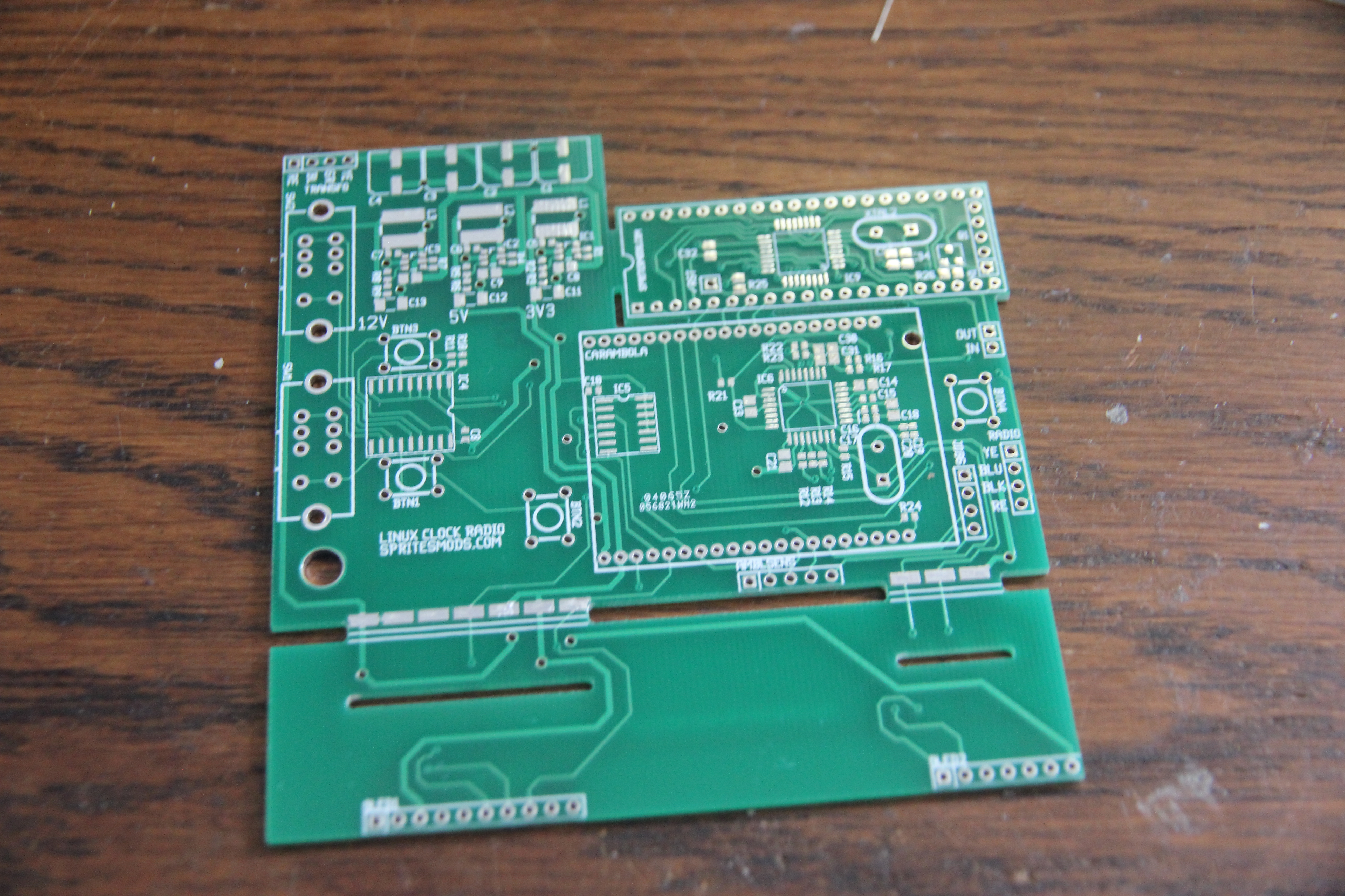
The front of the PCB is designed to be sawed off. The slots in it can then fit on the stubs that remain on
the other PCB.
The contacts on both PCBs can then be soldered, and this gives a fairly sturdy electrical and mechanical
connection between the two.
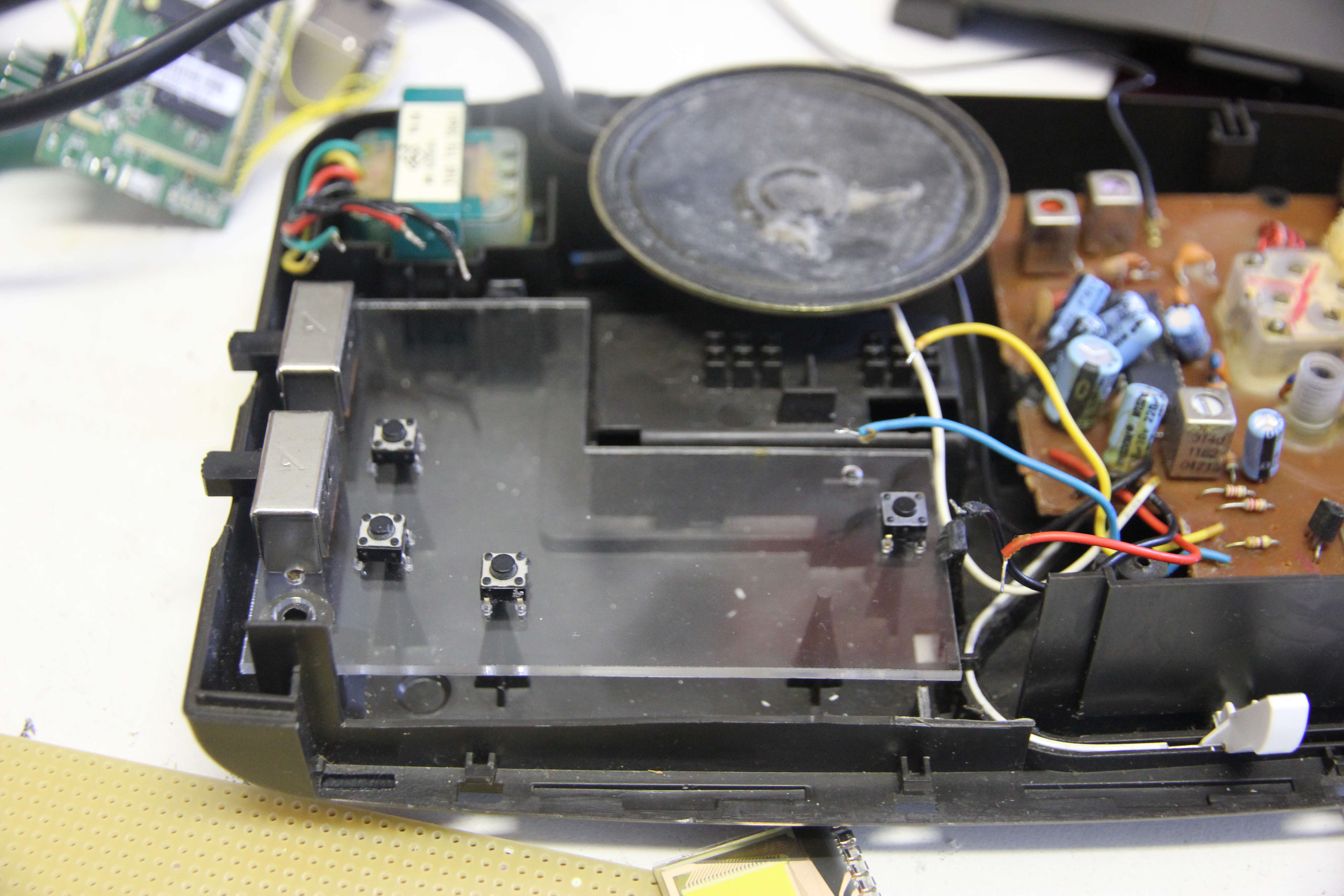
Now I would need to build the thing. Because this was somewhat of a rush job (and because in general it's good practice), I decided on building and testing the PCB one subsystem at a time.
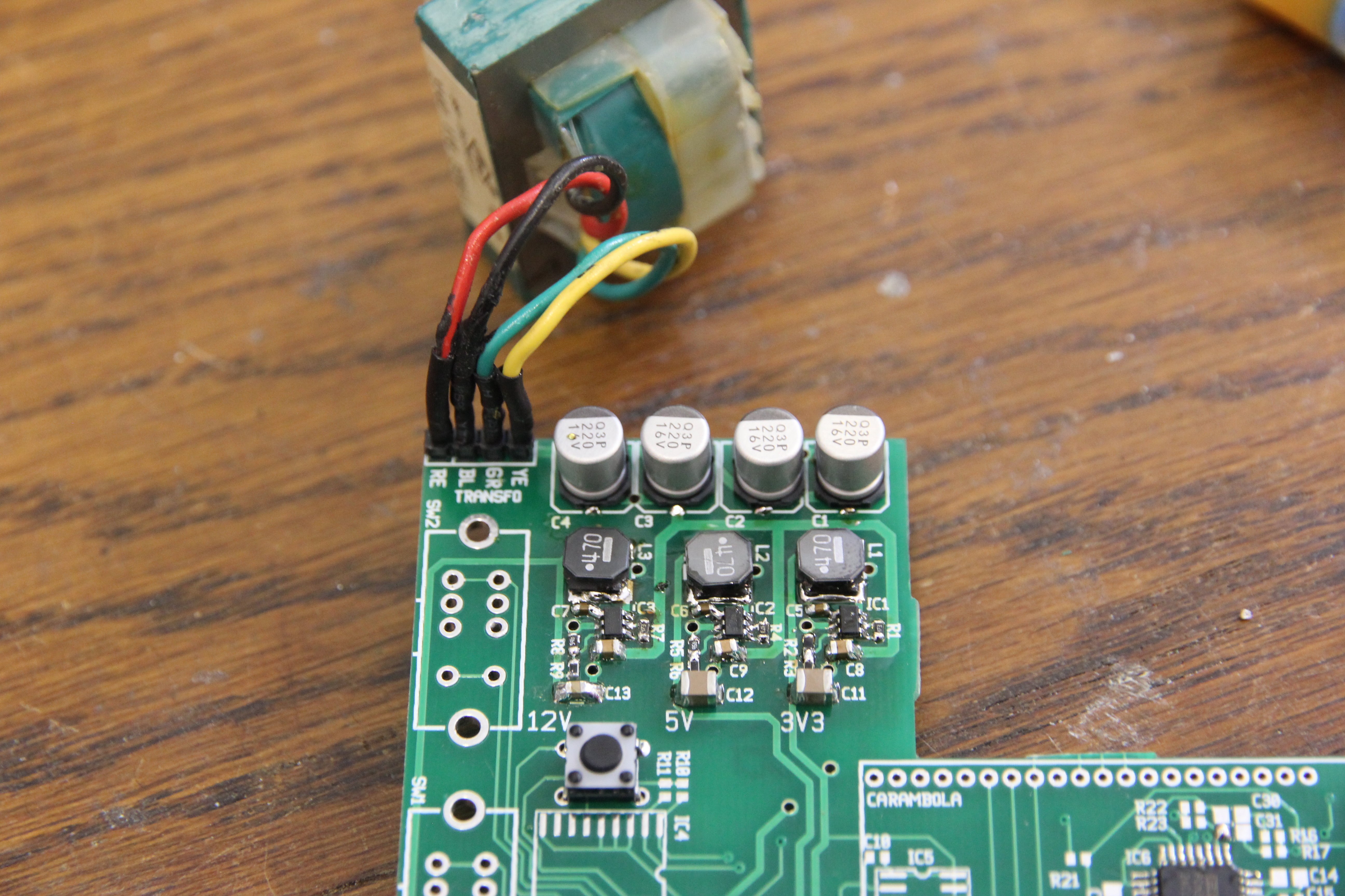
First came the power supply. I found I accidentally rotated a diode footprint 180 degrees there, but
after correcting that, everything worked: I got a nice and stable 5V, 12V and 3.3V.
Then came the USB sound card chip. The nice thing is that this is testable by just hooking it up to
an USB cable and plugging it in. Again a footprint error here: I managed to rotate the complete chip
by 90 degrees... Luckily, these ICs are quite sturdy (which is good, a chip is about 10 bucks) and
after de- and resoldering everything worked fine.
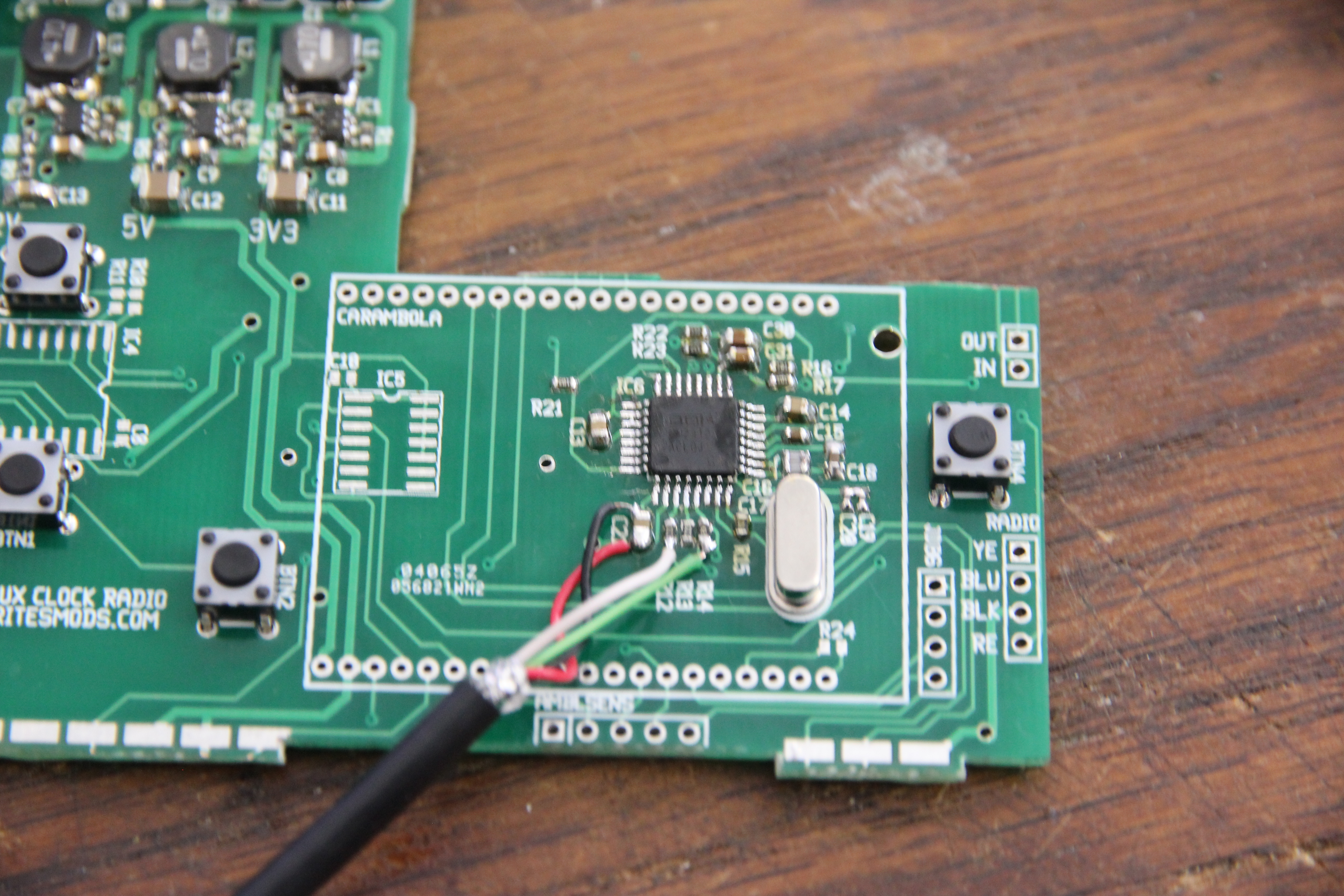
Then the rest: the I2C stuff, the Carambola and the OLED part. I also found some misc stupidities in the
design there, none that couldn't be fixed with a bodge wire though. It did make me quite happy to see
the old familiar Linux console booting on the OLED screen.
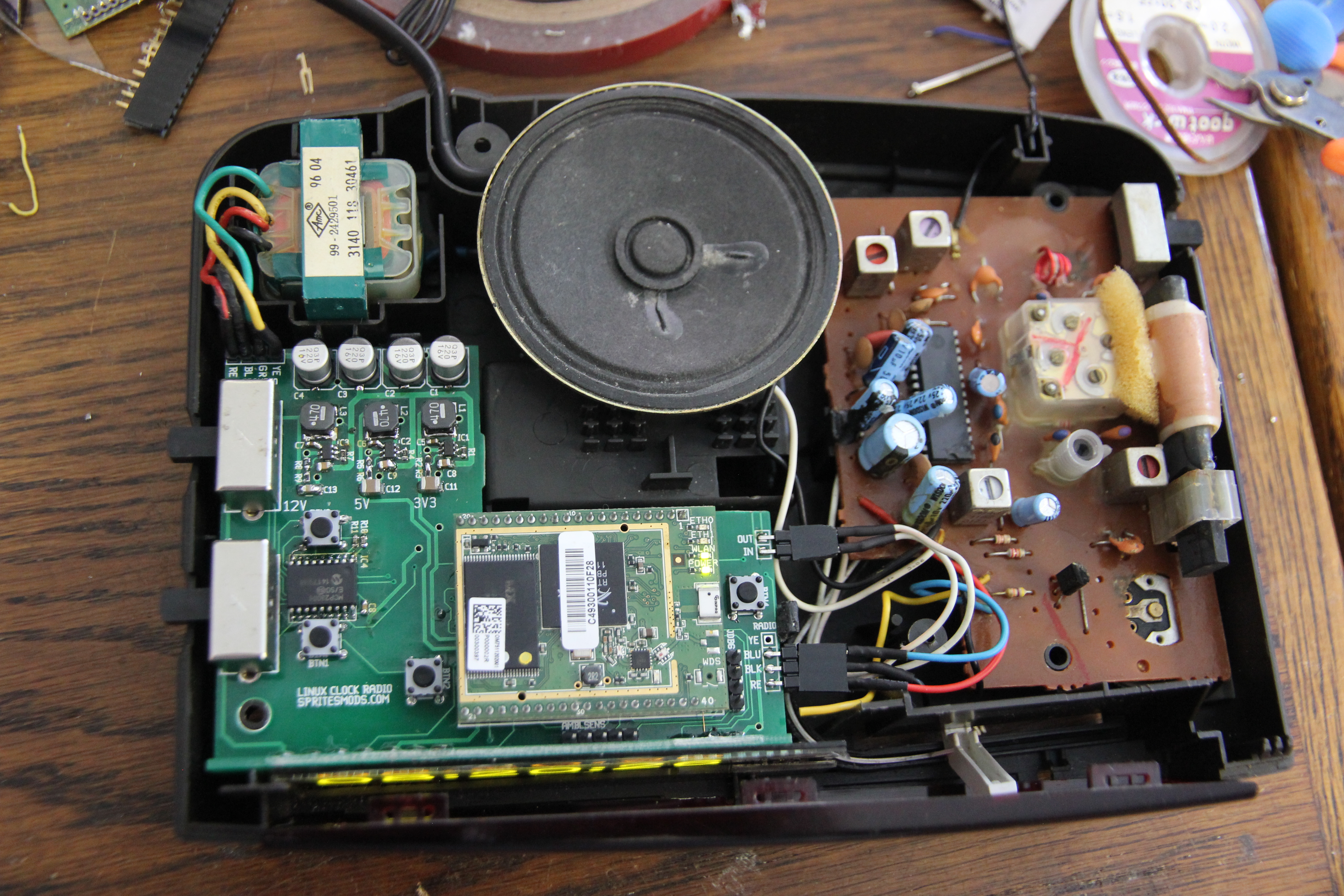
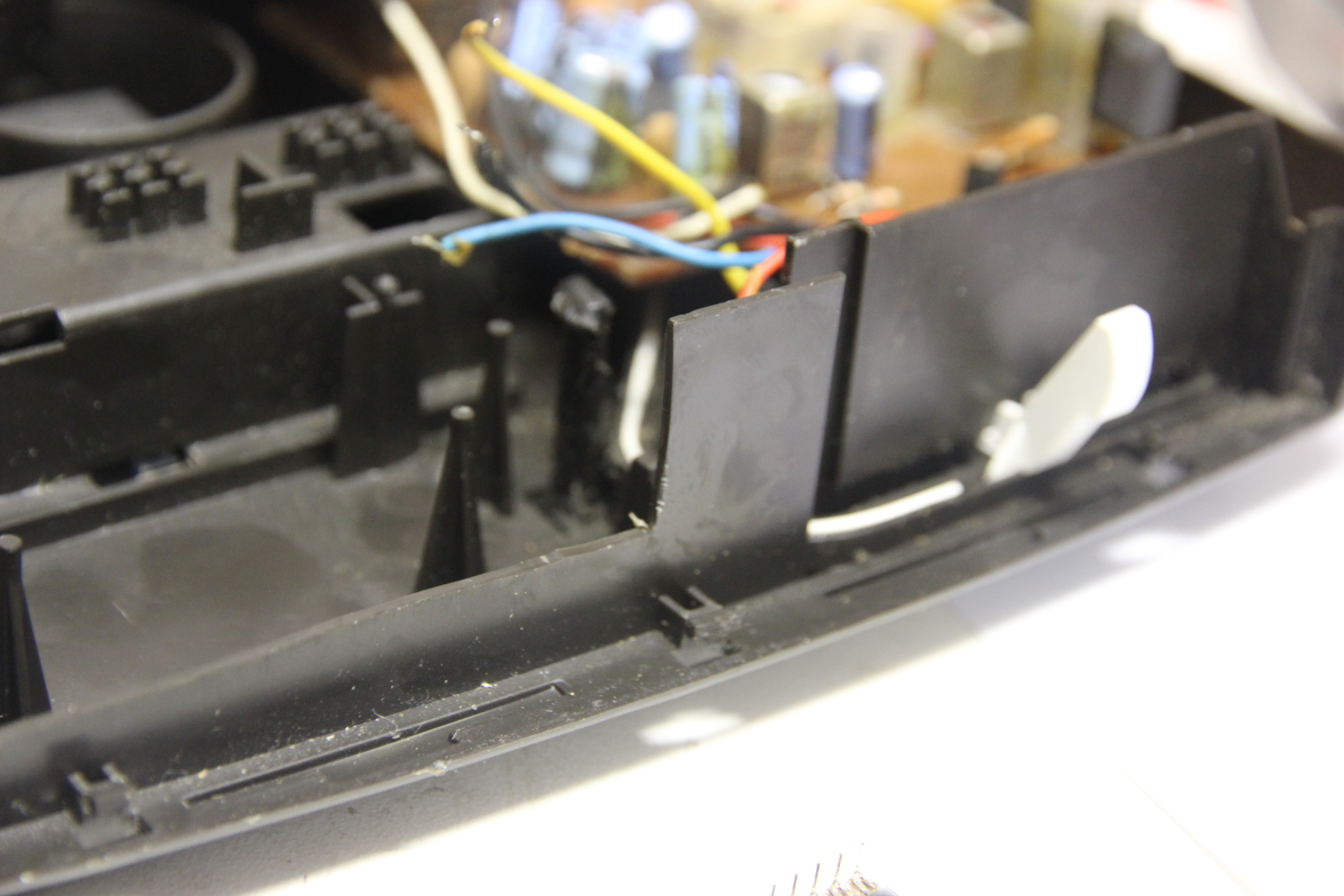
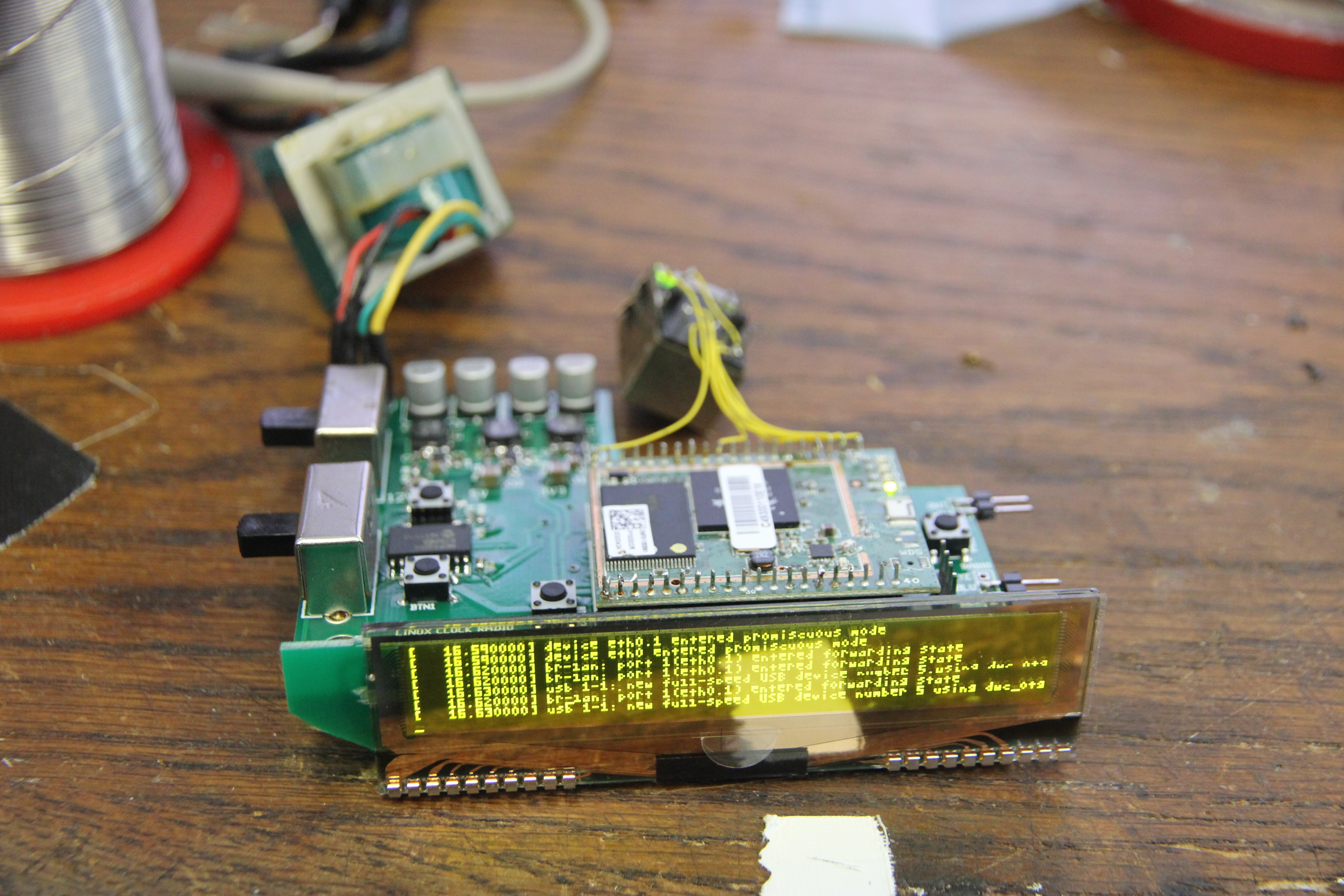
And with some work, everything managed to fit into the clock radio itself. I did need to make some small
modifications to make it work: for example the OLED display PCB had a corner that wouldn't fit in the case.
This could easily be solved by cutting it off; there were no traces or parts in that specific corner anyway.