Design
So, to make a device to push the config of a system over JTAG every time it's powered up, I needed a few things: a description of what JTAG commands to execute, somewhere to store that description, something to actually fetch the description from storage to push it out over JTAG, and a way to put a new description into that storage.
For the description type, I picked XSVF. This file format (the extension probably stands for Xilinx Serial Vector Format) is basically a stream of instructions on how to manipulate the logic behind the JTAG-pins. It's a bytecode version of the ascii-based SVF file format, but the files end up being quite a bit smaller.
To store this description, I decided on a 24P40, which is a piece of serial flash which can store 512KBytes of data. This should be enough for most FPGAs, and if needed it can be expanded by picking a larger piece of flash. It's obtainable in a nice 8-pins SMD package, so it's not big, and it can be reflashed over the same interface without needing weird voltages.
For the rest, I picked an ATTiny85 microcontroller. This little 8-pins beast has enough flash and RAM to contain both an XSVF player as well as the rest of the logic needed to read or write from the flash. I decided on implementing a software UART as a way to update the XSVF that's stored in the flash chip.
But SPI, JTAG and serial, all on the 5 IO-pins of the ATTiny85? Is that possible? Yes,
with a few caveats and tricks:
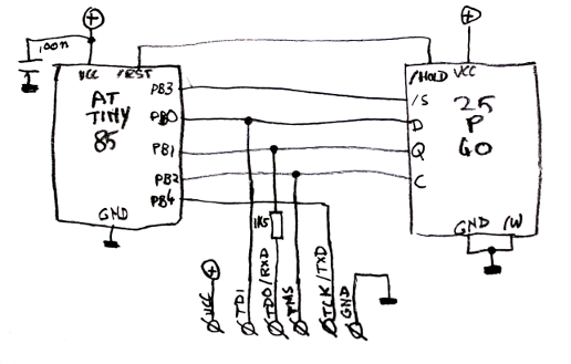
As you can see, a lot of pins are multiplexed and have multiple functions. How does
that work? Well, first of all I've decided to save me some headaches by deciding this
contraption will be used as a plug: either you connect it to a JTAG-connector, in which
case it will use the JTAG-pins to configure a device, or you want to update the
configuration and you plug it into a programmer header, which has the RxD and TxD
pins wired to a TTL-level serial port.
The rest of the pin sharing hinges on the fact that both JTAG and the flash will only care about what the values on their pins are in a special circumstance. For the JTAG, that's when the TCK-pin goed from low to high. That's when the JTAG logic samples the values on the other pins. With the TCK remaining in rest, it doesn't care what the levels on the other pins are, and because of the resistor, any value that's output on the pin of the serial flash will override whatever is on the TDO-line. The flash has something similar with its /S-input: when that line is low, the device will tristate its output line and ignore its input pins. Because the output pin Q is tristated, the AVR can now read TDO over this line.