Design
So as the video illustrated, the design goal of the DMGPlus was to put a Raspberry Pi in an authentic Game Boy in the most stealth way possible. That meant keeping in as much of the existing hardware as possible, and finding ways to interface with all of it: the display, buttons, cartridge, speaker, even the link port. Also, obviously, everything still needs to be powered from the 4 AA batteries that the original ran on.
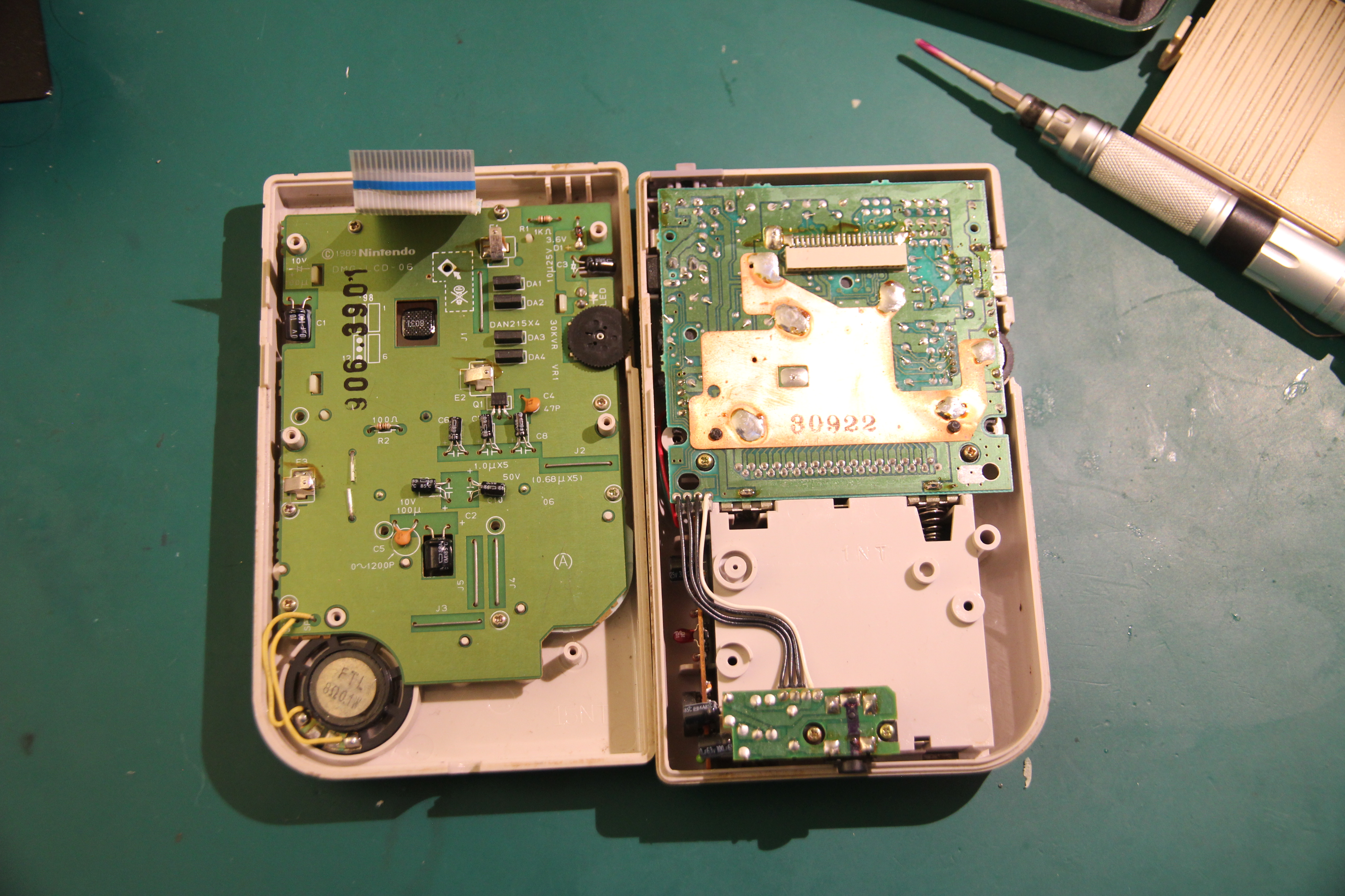
This is an original GameBoy, cracked open. There are four PCBs in total here: the large one on the left contains the display and button pads as well as the speaker. The somewhat smaller PCB on the right is the mainboard: it contains the processor, RAM, cartridge connector, link port, power button etc. There are two smaller PCBs under it: one contains the headphone connector, the other one is a power supply to convert the battery voltages to something usable for the rest of the logic.

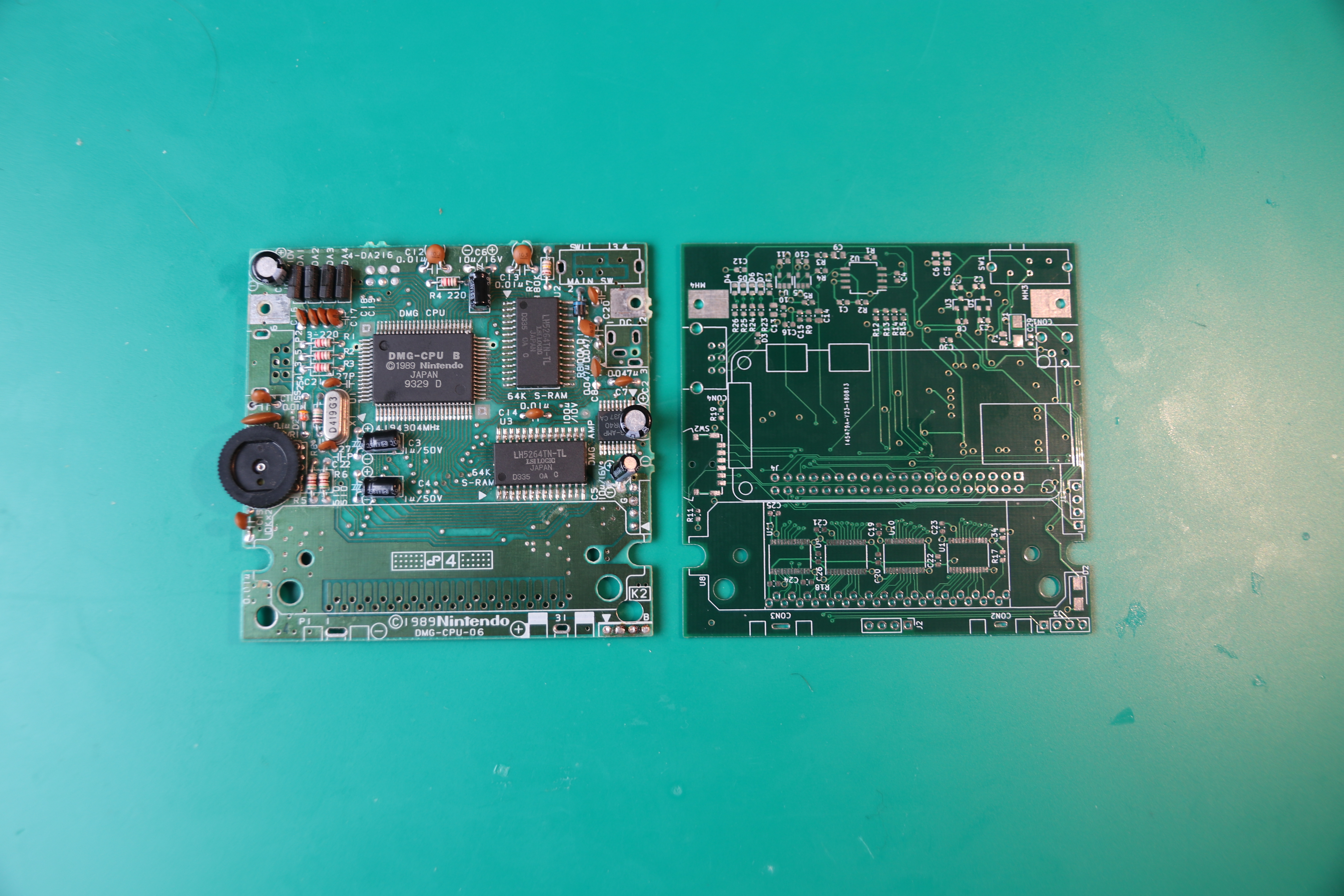
The other side. There's actually surprisingly little on the board, as Nintendo managed to cram everything in the man DMG-CPU chip. The only other chips on the board are two RAM chips and the audio amplifier.
Obviously, as the main board interfaces with everything else, it's a prime target for replacement; if I only replaced the main board, I could keep the rest of the GameBoy stock. This does mean that I need to put a fair few things on this board, however: the Raspberry Pi doesn't have that many pins, and out of the box it is not compatible with the signals the LCD needs. Aside from that, the GameBoy works on 5V logic levels and the Raspberry Pi uses 3.3V signalling. In order to fix this, we need a few things: a FPGA to do signal conversion and interfacing with things like the cartridge, as well as a handful of level shifters to go back and forth between signal levels.
I'll go through the schematic designs. Note that I added some bodges to the PCB as I went, and I sketched these into the schematic in blue.

Let's start with the core: the Raspberry Pi. In this case, it's a Raspberry Pi Zero W, as anything else than a Zero wouldn't fit, and the wireless is extremely useful in getting a remote console and files onto the device. This is needed as I didn't want to modify the GameBoy case and so the SD-card can only be removed by opening the GameBoy up.
The Raspberry Pi does not have audio output by itself, but the PWM pins on which the audio is generated are still there. All they need is an external filter network, something that already is integrated on the full-size Raspberry Pis. I later on bodged an extra audio input from the FPGA into this as well: as the Raspberry Pi takes some time to start up, the FPGA uses these lines to generate the familiar 'pli-ding!' bootup sound. The power supply rails was also beefed up with some ceramic caps, as I needed some more decoupling for the power lines.

The audio is then buffered by a pair of opamps that also work as a headphone amplifier. It's then send on to the headphone jack and the speaker amplifier. The headphone jack board also has an output to indicate if there's something plugged in, and this line is routed to the 'shutdown' pin of the amplifier. This way, the speaker stops when a pair of headphones is plugged in.

This is the FPGA. It's a Lattice ICE40, chosen because it's got plenty of IO and internal resources and there's a mature open-source toolchain for it. Ah, also because I had some in stock anyway. It is paired with a 512KByte SPI flash chip that contains its configuration. While it's technically possible to have the Raspberry Pi configure the FPGA on startup, I wanted the FPGA to be configured as as soon after power-up as possible, hence the flash chip.
The SPI bus for the flash chip is also connected to the Raspberry Pi. This serves a dual purpose, depending on the state of the FLASH_nCS line. If the line is low, the Raspberry Pi selects the flash chip and can reprogram it, which means that I can update the FPGA configuration from the command line. If the CS line is high, the configured FPGA is selected and the Raspberry Pi can talk to it to e.g. read out the cartridge port.
The Raspberry Pi is also connected to the FPGA using the DPI port. This port is a parallel interface consisting of red, green and blue signals and synchronization signals: the Raspberry Pi can use this as a native display port and you can e.g. connect a LCD or VGA adapter to it. Here, we use it to get the display signals of the Raspberry Pi into the FPGA, which can then convert them to something the GameBoy screen can process.
The FPGA is also connected to the GameBoy link port. I'm not entirely sure how a normal GameBoy would react to 3.3V signals and I also never wrote FPGA support for it, so it's non-functional in the current iteration of the project.

The GameBoy LCD is connected to the FPGA via a level shifter, and this possibly has the weirdest bodge of all. The GameBoy LCD is 5V, so we need a level shifter to take the 3.3V signals from the FPGA up to 5V levels. However, I found that with this setup, even when I got the timings right, the LCD refused to work properly: it flickered and generally acted up. This was until I measured the levels on the original mainboard again, and it turns out the 'low' levels are slightly above ground there. To replicate that, I use a diode to raise the ground level of the level converter ever so slightly, and it looked like this did the trick. I have no explanation for why this is needed, all I know is that since I did the mod, the display is rock solid.
The display connector also carries the signals for the GameBoy buttons. I added an input mechanism to this: instead of the volume potmeter, I put a rocker switch which you can tilt up and down and push. The idea is that I can sneak in a few extra 'buttons' this way if needed, while it still looks stock, and if I actually need to use this to be able to modify the volume, I can do that in software.

The FPGA is also connected to the cartridge connector, and as the GameBoy carts normally are also 5V things, a group of logic converters is used to convert the signal back and forth.

Finally, the power supply. The GameBoy can run off both four AA batteries as well as an external power supply via a barrel connector; the barrel connector itself switches between the two and a Schottky diode stops any charge leaking from it into the battery in case the mechanical switch is too slow. I've re-used the original DC/DC converter as it seems to work quite well, and aside from the 5V it also generates the negative bias voltage required for the LCD to work. As the 5V is only used for the level converters and the GameBoy components that were already there, it should have an easier job than in the original Game Boy.
The battery voltage goes via a diode straight into the 5V input of a Raspberry Pi. This is possible as the Raspberry Pi itself doesn't really use the 5V for anything; it feeds it straight into an on-board DC-DC converter to generate 3.3V and the other voltages it requires. The 6V that four AAs can generate could be a bit too much for that DC-DC converter, so D2 knocks the better part of a volt off that. The 3.3V that is generated by the Pi is also used to run the FPGA, but the FPGA also requires some auxiliary voltages. These are generated by a pair of tiny LDOs. Finally, as a bodge there's a pair of capacitors in parallel with the battery: without them, the Raspbery Pi had the tendency to brown out early when the batteries were running out of juice.
And here's the final PCB, next to the original one. I made it into a four-layer PCB; this made it the easiest to route all signals and keep a good ground- and powerplane. The idea was to keep the form factor as well as the locations for all the components that are accessible from the outside in the same spots, so the new PCB is a drop-in replacement. (I didn't quite succeed there; I mis-measured some holes for the cartridge connector, leading to some post-fabrication drilling and some more bodging of tracks, but with that mod, everything fits in place quite nicely.)
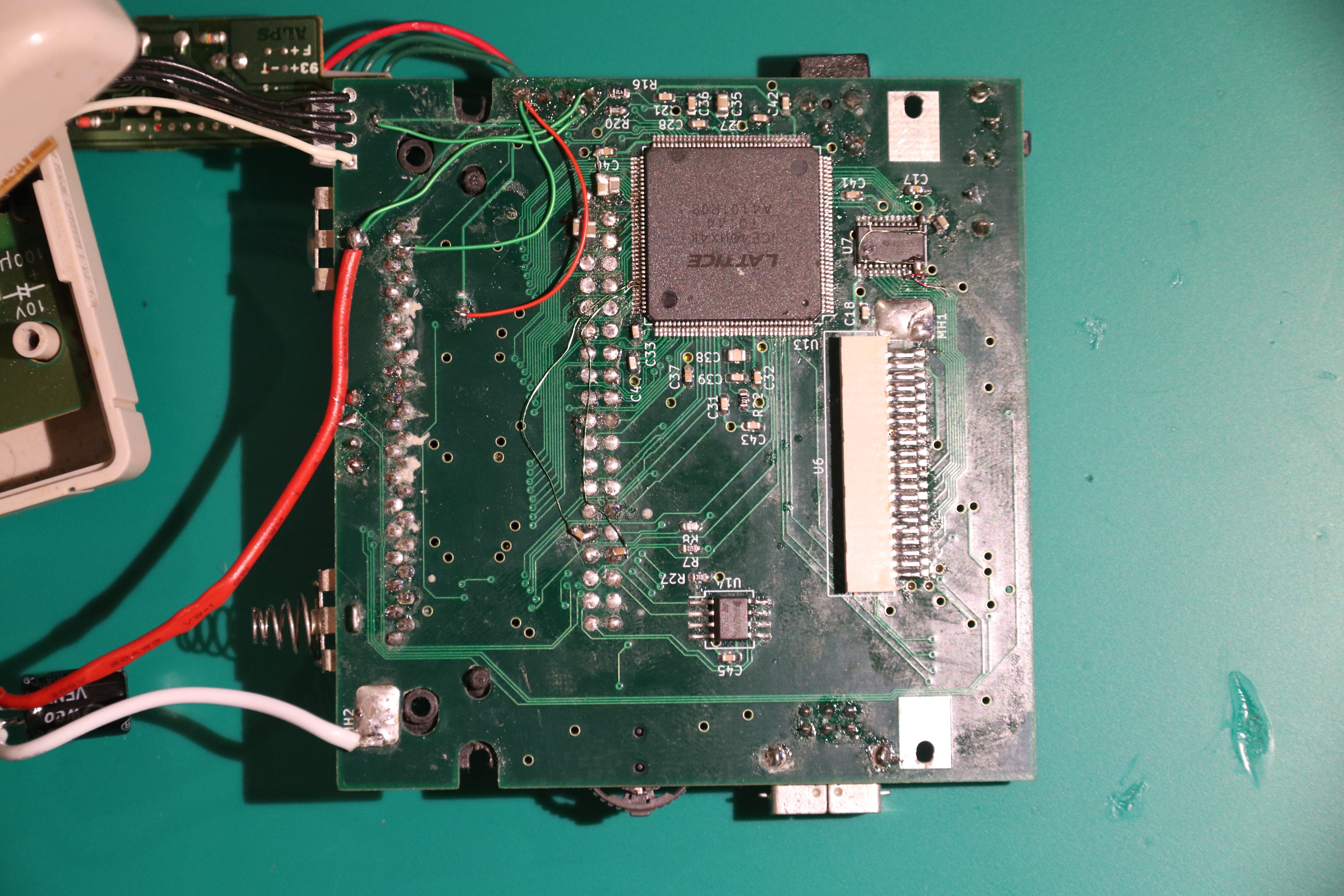
This is the front of the final PCB. You can see the aforementioned bodges in green on the top left. On this side you also can see the FPGA and the bodged LCD level shifter U7. The white flatcable connector is where the FPC to the LCD PCB connects to.
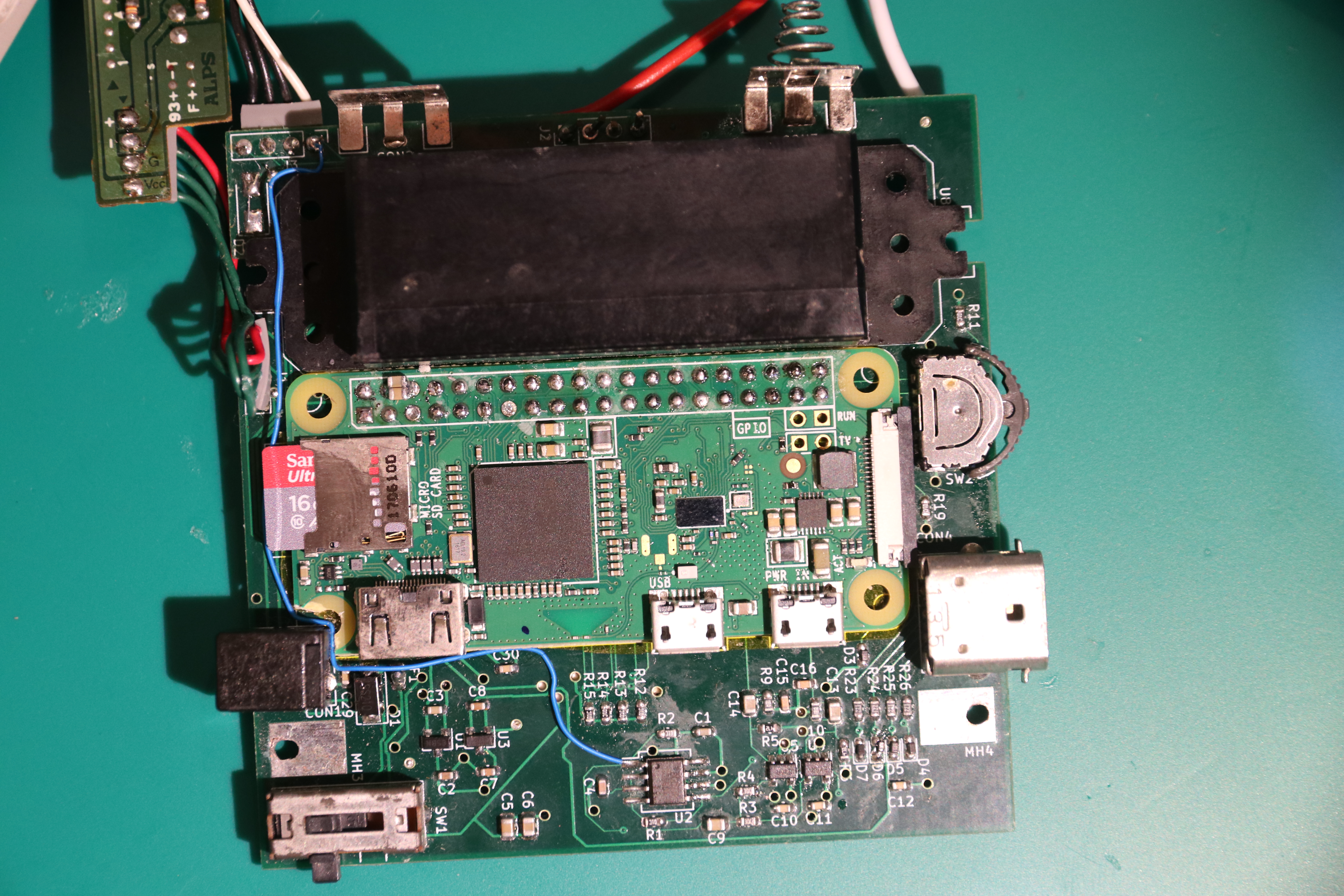
And here's the back. The Raspberry Pi is stuck onto the PCB using double sided tape, then the holes of both PCBs are connected by filling them with solder. There's no header used as that would make the entire sandwich too thick. Also note that one corner of the Raspberry Pi is cut off as it interferes with the power connector.
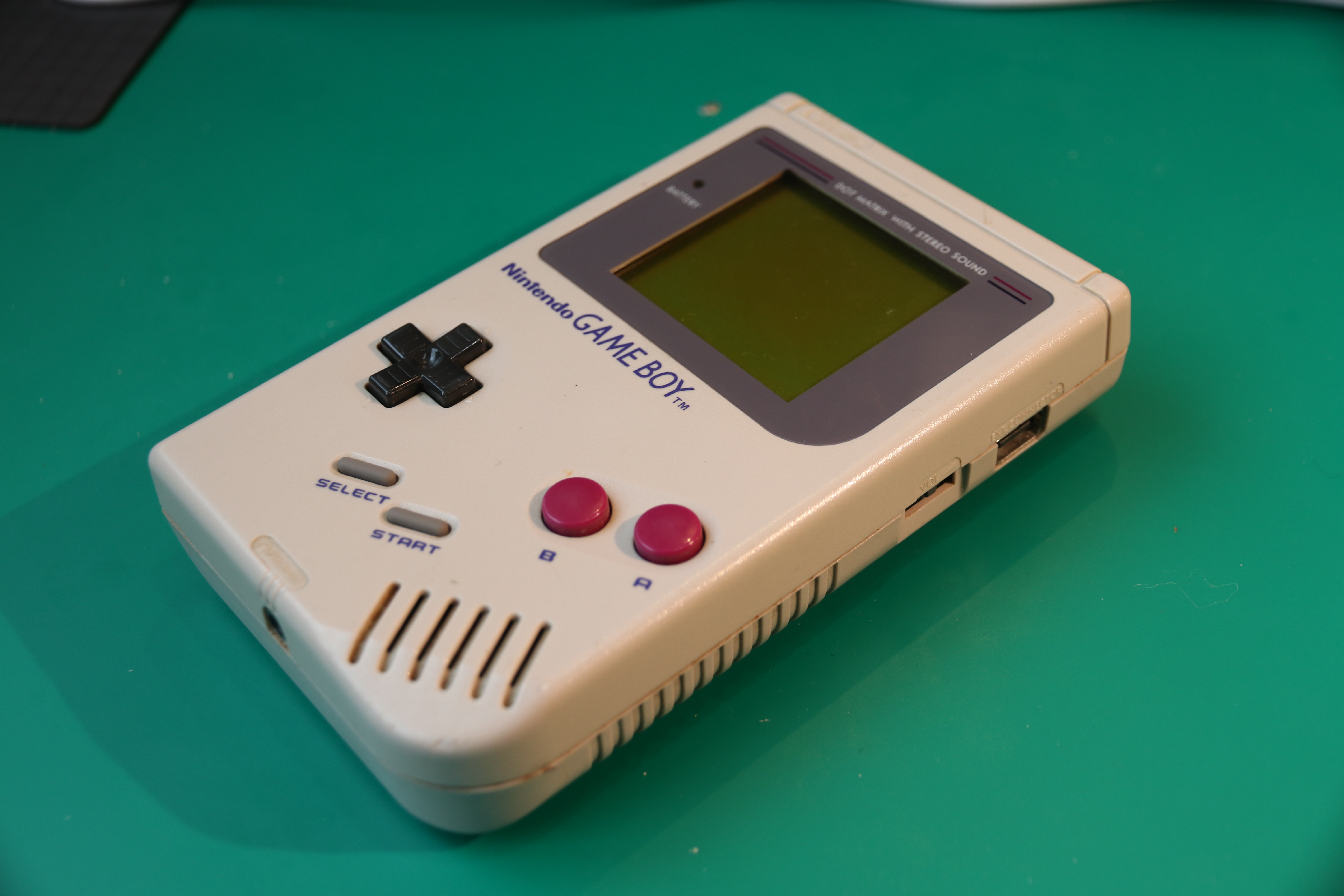
And here's the GameBoy back in its assembled form. The only way you could perhaps see that it's not stock is that the volume button doesn't look original anyore.