Soldering a WCSP package
The HC32L110 comes in a WCSP package. WCSP stands for Waver-level Chip Scale Package. The idea is that rather than packaging the actual silicon chip in plastic to get the DIP or TQFP chips you're used to, the chip simply gets some solder balls connected with it and that is that. These balls are mostly GPIO and peripheral IO pins, but there are a few balls that have a fixed function and need to be connected to specific voltages and external components in order for the chip to work and be programmable:

The issue here is that because WCSP chips are made to have almost no superfluous case, it's as small as it can get, not larger than the silicon die itself. This also means the external connections need to be small, as they all need to fit on that surface. In this particular case, the chip has 16 solder balls with a distance of a mere 0.35mm between them.
Not anything us mere mortals can do anything with, right? You'd need super-expensive PCBs to connect to that and the package is impossible to solder by hand, right?Well... that's not necessarily true. For instance, even the cheapest 2-layer process that JLCPCB offers is capable of 0.127mm tracks spaced 0.127mm apart... which means you can lay down tracks at a minimum of 0.254mm apart. That's good enough to connect to pads with a 0.35mm pitch.
But what about vias? Well, that's true, the minimum via diameter is 0.4mm, so there's no chance at all to put any of those under the chip. And as we also do not have the clearance to sneak out a trace between chip balls, there's no way to connect the inner four pads of the chip to the outside. Which is a shame because some of those are quite important: the reset pin and the capacitor for the internal core LDO connect to that. That means we can't use the chip, right?
Well, in this particular case there is a workaround. Most of the outer pins are GPIOs; they are configured as inputs on reset, which means that unless software reconfigures them, they won't actively source or sink current. That means that if we connect an inner pin through a GPIO, the GPIO will not affect the signal of that inner pin as long as we let it be an output. In other words: as long as we give up some pins on the outside of the package, we can still get to the signals on the inner pins. Also note that I only used the small trace size to get to the pads, where it's actually necessary: as any trace that is close to the limits of the board houses capabilities has a chance of not being manufactured correctly, I tried using as little trace length that is minimum-width as possible

It may be worth mentioning that there is another alternative, in case you need to run a trace through an unused pin that can't be put in high-impedance mode: you can simply remove that pad in the footprint and make sure the trace that runs there is covered with solder mask or even silkscreen. The downside of that here is that solder mask and silk screen do have some thickness to it, and it may lead to the unused solder ball being squished into its neighbours, hence I didn't use it here.
Either approach means we only lose access to four pins, and with the PCB design I chose, soldering the chip to the PCB is actually fairly easy with a microscope, cheap hot-air rework station, some flux, tweezers and some patience.
Now obviously, the fact that this gives us only 12 of the 16 pads is a bit of a shame. The only way to get those extra pads is to use an extra-expensive PCB manufacturing process that uses either microvias or can route tracks between the pads... or you could cheap out and do something crazy like dead-bugging the chip.
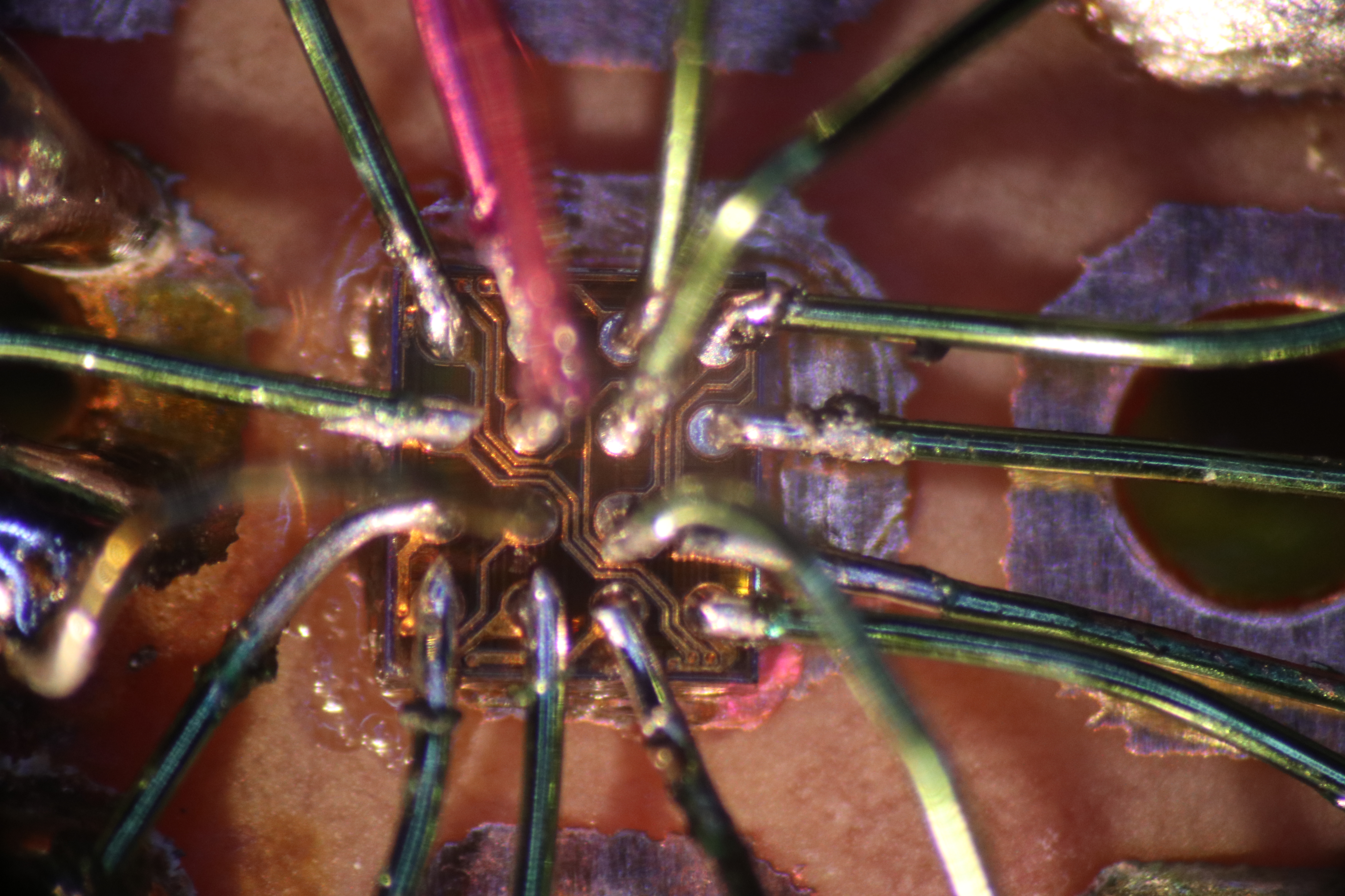
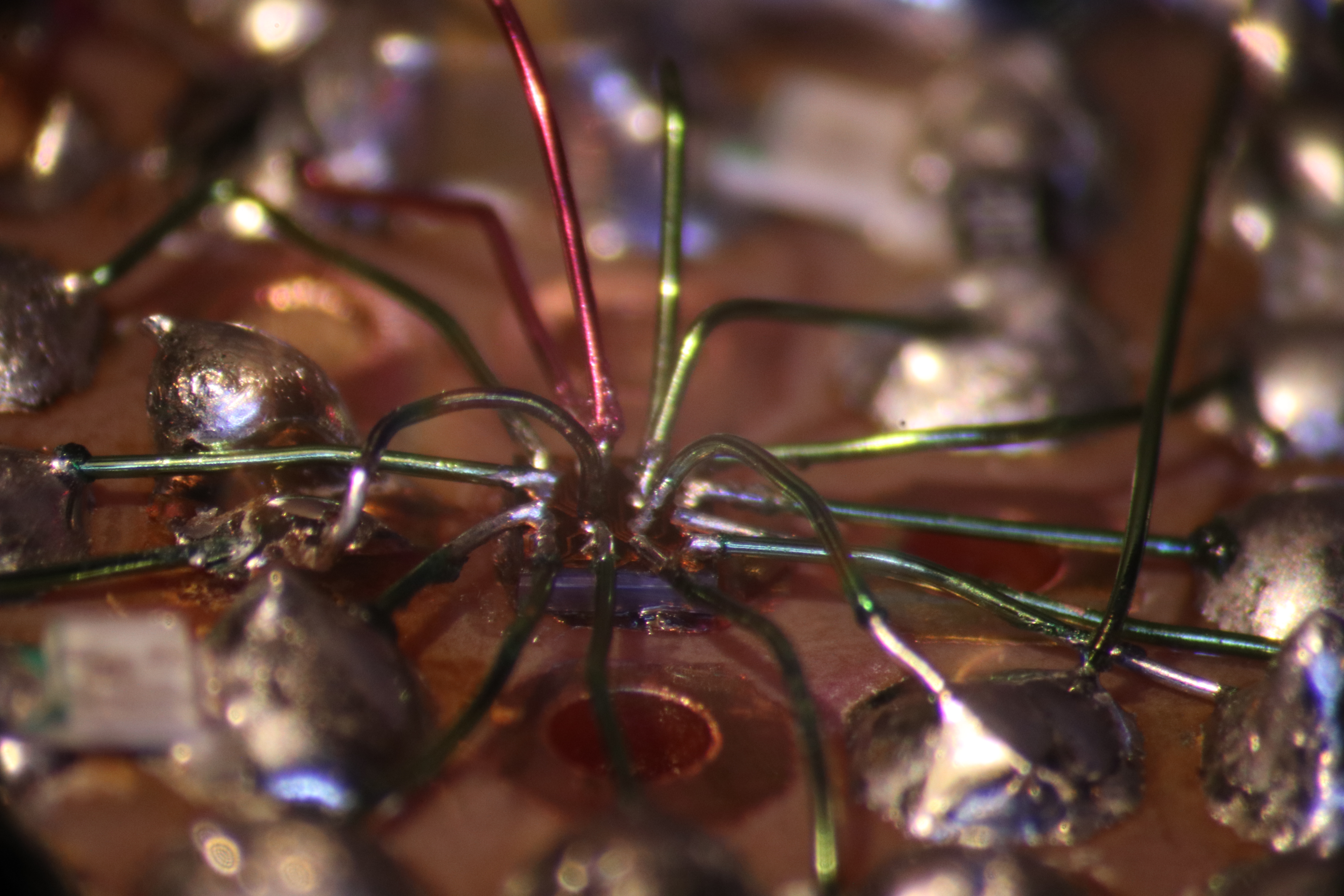
(And yes, that chip actually works. There's still a livestream capture online of me soldering it.)
So now the chip is soldered; all we need to do is to program the obligatory blink program into it. If we can figure out how to compile and program one...