Hooking up JTAG
Luckily, there are other ways to find out information about these ICs than datasheets. One of my web searches actually resulted in something useful.
what I found was a thread from a guy called Dejan on the HDDGuru forums. Dejan had managed to corrupt the internal flash of his hard disk in some way and wanted to know if there's a way to either boot the controller from external flash, or a method to re-write the flash. For five days, he doesn't get a reponse, but the guy is inventive: the next thing he posts is the message that he has found the pinout of the JTAG-port. That's a major find: the JTAG-port can be used to control a controller like a puppet. You can stop it, restart it, modify memory, set breakpoints etc with it. Dejan then figures out how to dump the boot ROM of the controller, figures out there's a serial port on one of the hard disk headers and manages to restore his flash ROM. He then dumps a few more bits and pointers about the flash update process before finally disappearing into the mists of the Internet again.
All this was pretty useful information: it told me at least the Western Digital controllers seem to have an ARM-core that's accessible over the JTAG-port. It also told me these hard disks usually have a serial port, which is usually unused but could be useful for debugging my hack. With this, I should have enough information to start hacking.
So, this is my setup:
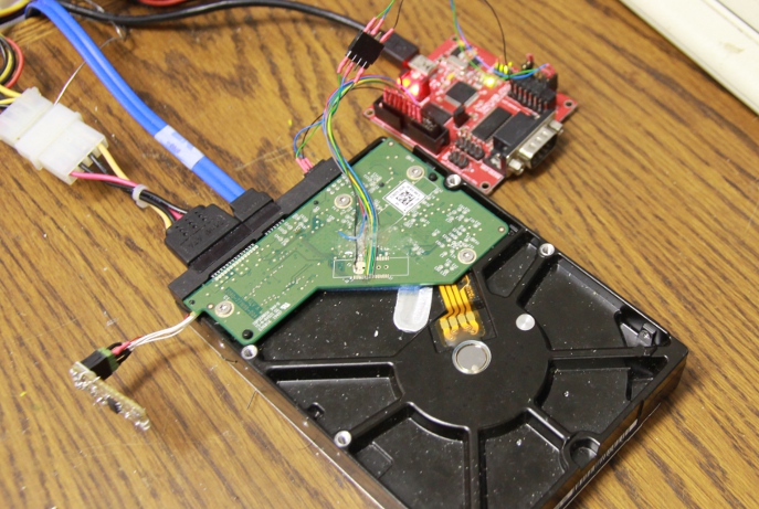
The red thing is an FT2232H-board, a cheap board you can get for about EUR30 which can do JTAG and serial, as well as SPI-communications. It's connected to the JTAG-interface of the hard disk, as well as the header where the hard disk has its serial port. The HD is directly connected to the SATA-port on my computers mainboard, as well as to an external ATX power supply. I use OpenOCD as the software to drive the JTAG-port.
Now, the question is: would it actually work? Dejan did this with
a 2.5" 250G HD with an 88i6745-controller, and he detected an arm9-core.
I grabbed a 3.5" 2TB HD with an 88i9146-controller instead, which had
a different form factor and is a bit newer. Luckily, OpenOCD has a way
to detect what's on the JTAG chain by itself. This is what it found:

This confused me for a bit... I expected a single tap, for the single ARM core that's inthere... but instead, I found three taps... does that mean this chip has three ARM-cores?
After some research, I found out that yes, the chip indeed seems to have three cores. There's two Feroceons, which are quite powerful arm9-like cores, and a Cortex-M3 core, which is a bit smaller, more microcontroller-ish core. Some more playing around (and later research) indicating the controllers all had different functions:
- Feroceon 1 handles the physical reading and writing from/to the hard disk platters
- Feroceon 2 handles the SATA-interface
- Feroceon 2 also handles the cache and LBA to CHS translation
- The Cortex-M3 handles... nothing? I could stop it and still have all hard disk functions.
Now, what core to start hacking at? My target was to try and compromise the security of a system by using hard disk firmware mods. The easiest and probably hardest-to-detect way to do this was to modify data on the fly. That way, the data on the disk wouldn't need to be changed and the firmware could just make itself invisible. To do this, I would need to find a suitable core to that kind of interception: I needed to have a core that would have access to the data when it's in-transit from the disk to the SATA-cable, and also could be rigged to modify the data while it was in between those two points.
Now, how would that data get from the HD platters to the SATA interface?
Here's where I used a bit of intuition. My reasoning went something
like this:
If the processors would use a standard memory copy, with them running
at 150MHz, they would only be able to reach 150*23/2=2.4Gbps, and in
practice most likely much less. The hard disk is specced at 6Gbps, so
there's probably some hardware acceleration involved. The most likely
hardware acceleration would be to use DMA. That would mean the data
is copied directly from the head reading logic to memory, without
active involvment of the processor. The same goes for the SATA-port:
the processor would have to only indicate where the data is, and the
DMA logic would take care of reading the data directly from memory.
If this was the case, where would the memory that the DMA-engine would be pointed at, be located? The cache of the hard disk would be a good location: data read from the disk would need to be in cache anyway, so it would make sense to copy it there immediately when reading from the disk. I figured out earlier that Feroceon 2 was responsible for the cache handling; that'd make it a prime target for a hacking attempt.
So, I deduced that the data was read and written through DMA, without
any CPU action involved. Now the question was: Even if the CPUs
won't touch the data in normal operation, can they
actually access it? To answer this question, I first used the
JTAG-connection and a bit of disassembly to figure out the memory map
of the 2nd Feroceon:
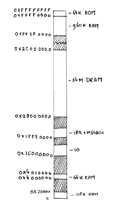
As you can see, the memory map is a bit fragmented. There are small bits of RAM sprinkled around, there's some IO and IRQ space, and a bit of internal boot ROM. There also is a big, 64MB segment of what I suspected was the DRAM-chip with the cache in it. Let's find out if this is actually true. First, I mounted the disk on my machine and wrote 'Hello world!' to a file on it. Now, could I find the string in the 64MB mem region?
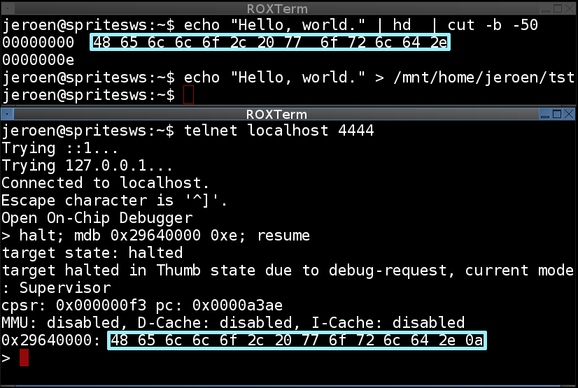
Yep, there it is. Seems the cache is accessible by the Feroceons and mapped to the 64MB DRAM region.