Driving the display
While I had nothing to complain about the resolution, size and brightness of the display, actually getting pixels to it was more problematic. The MIPI interface it has was not supported by the ESP32 silicon so I would have to find another way to interface with it. The MIPI DSI interface is a standard developed by the MIPI Alliance and not public; as a hobbyist, I'd have to piece together the details from leaked documents and probing of existing devices. Luckily, a year or two ago Mike Harrison reverse engineered the MIPI DSI interface used to control iPod displays (1, 2, 3, 4, 5, website) and also managed to find some copies of the specifications. This made my life a lot easier: it helps to at least know what to send to the display.
While there is a lot more to it (and you should really watch the above videos if you want to know what), the
physical layer of the MIPI protocol is pretty simple to explain. The MIPI protocol uses four wires in total: two
data- and two clock-lines. The MIPI protocol has two modes of signalling: Low Power (LP) mode and High Speed (HS)
mode.
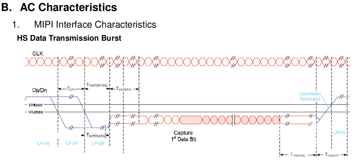
In Low Power mode, the wires are used separately to transmit some control data structures as well as indicate certain commands that have direct effect on the physical receiver on the other side. The voltage swing in this mode is pretty large compared to the high speed mode: voltages are either around 1.2 volt for a high signal, or around 0 volt for a low signal. Because low speed mode has more signal states, it does things like tell the receiver to enter or exit high speed mode. In the diagram above, the blue lines indicate Low Power communication.
In High Speed mode, the two clock lines (CLKP/CLKN) as well as the two data lines (DP/DN) work as differential lines, with one line always being the opposite as the other one. The receiver detects the difference between the two lines, and deduces the value being sent from this: a 1 if DP is higher, a 0 if DN is higher. High-speed mode, as the name implies, allows for very quick data transfers with clocks up to 1.5GHz. The trick the standard used to get this done without too much EMC and power use is to use very low voltages in this mode: the voltages on the pairs average to about 200mV, with variations of +/- 100mV per line to indicate the ones and zeroes. In the above diagram, the red bits are done in high-speed mode.
For the actual data transfer, in high speed mode the interface can essentially be seen as a somewhat weird and differential SPI interface: there is a clock and data path, and every clock tick, the value of the data is clocked into the interface. A change from SPI, apart from the fact that the signals are differential, is that a data bit is clocked in whenever the CLK lines change state, instead of only on e.g raising edges. Another difference is that the start of a transfer is detected not by a /CS line going low, but by in-band signalling: every transmission starts with one unique binary 'magic word' and the receiver detects this value to decide when a transmission starts.
In order to interface this with the ESP32, I'd have to do some level shifting. I wanted to run the ESP32 from a 3.0V power source, so all GPIOs would also be 3.0 or 0 volt. To adapt this to the signal levels of the MIPI interface, I opted for the most cheap solution: just use some resistor divider networks.
To figure out the resistor values, I effectively made equations for the three voltage output states that
interested me (1.1V for Low Power high, 0.07V for High Speed low, 0.33V for High Speed high; voltages chosen
to stay in-spec for most situations) and the three input states that should generate them. Using some math,
I ended up at some equations. I could theoreticaly work out those equations by hand, but eventually decided
to throw them into WolframAlpha which gave me the needed resistor
values.
           3V
G -R1--+   R3
G -R2--+ --+---->
           R4
           GND

R4*(1.9/R1+1.9/R3)=1.1,
(1/(1/R4+1/R1+1/R2))*(2.93/R3)=0.07,
(1/(1/R4+1/R1))*2.67*(1/R3+1/R2)=0.33,
R2=1000

R1=280, R2=1K, R3=3K6, R4=150
At that time, I figured I could also cheat a bit: because the lines are differential in high-speed mode, the
display will only look at the difference between the two lines to deduce the data sent. This means that I can save
a GPIO by holding one of the lines at a fixed voltage, making the other line higher and lower as needed. To do this,
I needed a second type of resistor network:
           3V
           R3
G -R1--+ --+---->
           R4
           GND

R4*(1.9/R1+1.9/R3)=1.1,
(1/(1/R4+1/R1))*(2.8/R3)=0.2,
R4=150

R1=320, R3=1500, R4=150
Another thing to solve was the clocking scheme. Normal SPI clocks in a bit on a raising edge of the clock line. (Or a falling one, depending on the configuration.) MIPI clocks in a bit on both the raising as well as the falling edge of the clock signal. While the ESP32s hardware SPI unit cannot by itself generate a signal like this, we can convert from one to another by using a simple D-type flipflop with its inverted output connected to its input. Every clock pulse on the input will change the level of the output, exactly as is needed here.